ZHCSBE0C August 2013 – August 2015 UCC27517A
PRODUCTION DATA.
9 Detailed Description
9.1 Overview
The UCC2751xA single-channel, high-speed, low-side gate-driver device is capable of effectively driving MOSFET and IGBT power switches. Using a design that inherently minimizes shoot-through current, the UCC2751x device is capable of sourcing and sinking high peak-current pulses into capacitive loads offering rail-to-rail drive capability and extremely small propagation delay of 13 ns (typical). The UCC2751xA family of devices provides 4-A source, 4-A sink (symmetrical drive) peak-drive current capability. The device is designed to operate over a wide VDD range of 4.5 to 18 V, and a wide temperature range of –40°C to 140°C. Internal undervoltage lockout (UVLO) circuitry on the VDD pin holds the output low outside VDD operating range. The capability to operate at low voltage levels, such as below 5 V, along with best-in- class switching characteristics, is especially suited for driving emerging wide bandgap power-switching devices such as GaN power-semiconductor devices.
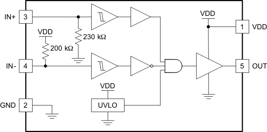
The UCC27517A device features a dual-input design which offers flexibility of implementing both inverting (IN– pin) and non-inverting (IN+ pin) configuration with the same device. Either the IN+ or IN– pin can be used to control the state of the driver output. The unused input pin can be used for enable and disable functions. For system robustness, internal pull-up and pull-down resistors on the input pins ensure that outputs are held low when the input pins are in floating condition. Therefore the unused input pin is not left floating and must be properly biased to ensure that driver output is in enabled for normal operation.
The input pin threshold of the UCC27517A device is based on TTL and CMOS-compatible low-voltage logic which is fixed and independent of the VDD supply voltage. Wide hysteresis between the high and low thresholds offers excellent noise immunity.
Table 2. UCC27517A Summary
| PART NUMBER | PACKAGE | PEAK CURRENT (SOURCE, SINK) | INPUT THRESHOLD LOGIC |
|---|---|---|---|
| UCC27517ADBVQ1 | SOT-23, 5 pin | 4-A, 4-A (Symmetrical Drive) |
CMOS and TTL-Compatible (low voltage, independent of VDD bias voltage) |
Table 3. UCC27517A Features and Benefits
| FEATURE | BENEFIT |
|---|---|
| High Source, Sink Current Capability 4 A, 4 A (Symmetrical) | High current capability offers flexibility in employing the UCC27517A to drive a variety of power switching devices at varying speeds |
| Best-in-class 13-ns (typ) Propagation delay | Extremely low-pulse transmission distortion |
| Expanded VDD Operating range of 4.5 V to 18 V | Flexibility in system design Low VDD operation ensures compatibility with emerging wide-bandgap power devices such as GaN |
| Expanded Operating Temperature range of –40°C to 140°C (See Recommended Operating Conditions table) |
|
| VDD UVLO Protection | Outputs are held low in UVLO condition, which ensures predictable glitch-free operation at power up and power down |
| Outputs held low when input pins (INx) in floating condition | Protection feature, especially useful in passing abnormal condition tests during protection certification |
| Ability of input pins to handle voltage levels not restricted by VDD pin bias voltage | System simplification, especially related to auxiliary bias supply architecture |
| CMOS and TTL compatible input threshold logic with wide hysteresis in UCC27517A | Enhanced noise immunity, while retaining compatibility with microcontroller logic-level input signals (3.3 V, 5 V) optimized for digital power |
| Ability to handle –5 VDC at input pins | Increased robustness in noisy environments |
9.2 Functional Block Diagram

9.3 Feature Description
9.3.1 VDD and Undervoltage Lockout
The UCC27517A has internal Undervoltage Lockout (UVLO) protection feature on the VDD-pin supply-circuit blocks. Whenever the driver is in UVLO condition (for example when VDD voltage is less than VON during power up and when VDD voltage is less than VOFF during power down), this circuit holds all outputs LOW, regardless of the status of the inputs. The UVLO is typically 4.2 V with 300-mV typical hysteresis. This hysteresis helps prevent chatter when low VDD – supply voltages have noise from the power supply and also when there are droops in the VDD-bias voltage when the system commences switching and there is a sudden increase in IDD. The capability to operate at low voltage levels such as below 5 V, along with best-in-class switching characteristics, is especially suited for driving emerging GaN wide-bandgap power-semiconductor devices.
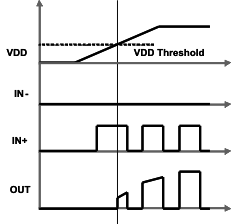
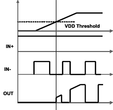
For example, at power up, the UCC27517A driver output remains LOW until the VDD voltage reaches the UVLO threshold. The magnitude of the OUT signal rises with VDD until steady-state VDD is reached. In the non-inverting operation (PWM signal applied to IN+ pin) shown in Figure 19, the output remains LOW until the UVLO threshold is reached, and then the output is in-phase with the input. In the inverting operation (PWM signal applied to IN– pin) shown in Figure 20 the output remains LOW until the UVLO threshold is reached, and then the output is out-phase with the input. In both cases, the unused input pin must be properly biased to enable the output. Note that in these devices the output turns to high-state only if IN+ pin is high and IN– pin is low after the UVLO threshold is reached.
Because the driver draws current from the VDD pin to bias all internal circuits, for the best high-speed circuit performance, two VDD bypass capacitors are recommended to prevent noise problems. The use of surface-mount components is highly recommended. A 0.1-μF ceramic capacitor should be located as close as possible to the VDD to GND pins of the gate driver. In addition, a larger capacitor (such as 1 μF) with relatively low ESR should be connected in parallel and close proximity, in order to help deliver the high-current peaks required by the load. The parallel combination of capacitors should present a low impedance characteristic for the expected current levels and switching frequencies in the application.
 Figure 19. Power-Up (Non-Inverting Drive)
 Figure 20. Power-Up (Inverting Drive)
9.3.2 Operating Supply Current
The UCC27517A features very low quiescent IDD currents. The typical operating-supply current in Undervoltage-Lockout (UVLO) state and fully-on state (under static and switching conditions) are summarized in Figure 6, Figure 6 and Figure 7. The IDD current when the device is fully on and outputs are in a static state (DC high or DC low, refer Figure 5) represents lowest quiescent IDD current when all the internal logic circuits of the device are fully operational. The total supply current is the sum of the quiescent IDD current, the average IOUT current due to switching and finally any current related to pullup resistors on the unused input pin. For example when the inverting input pin is pulled low additional current is drawn from VDD supply through the pull-up resistors (refer to Detailed Description for the device Block Diagram). Knowing the operating frequency (fSW) and the MOSFET gate (QG) charge at the drive voltage being used, the average IOUT current can be calculated as product of QG and fSW.
A complete characterization of the IDD current as a function of switching frequency at different VDD bias voltages under 1.8-nF switching load is provided in Figure 15. The strikingly-linear variation and close correlation with theoretical value of average IOUT indicates negligible shoot-through inside the gate-driver device attesting to the high-speed characteristics of IOUT.
9.3.3 Input Stage
The input pins of the UCC27517A are based on a TTL and CMOS compatible input-threshold logic that is independent of the VDD supply voltage. With typical high threshold = 2.2 V and typ low threshold = 1.2 V, the logic-level thresholds can be conveniently driven with PWM-control signals derived from 3.3-V and 5-V digital-power controllers. Wider hysteresis (typically 1 V) offers enhanced noise immunity compared to traditional TTL-logic implementations, where the hysteresis is typically less than 0.5 V. These devices also feature tight control of the input-pin threshold-voltage levels which eases system-design considerations and ensures stable operation across temperature. The very low input capacitance on these pins reduces loading and increases switching speed.
The device features an important protection function wherein, whenever any of the input pins are in a floating condition, the output of the respective channel is held in the low state. This is achieved using VDD-pullup resistors on all the inverting inputs (IN– pin) or GND-pulldown resistors on all the non-inverting input pins (IN+ pin), (refer to Functional Block Diagram section).
The device also features a dual-input configuration with two input pins available to control the state of the output. The user has the flexibility to drive the device using either a non-inverting input pin (IN+) or an inverting input pin (IN–). The state of the output pin is dependent on the bias on both the IN+ and IN– pins. Refer to the input/output logic truth table (Table 4) and the Typical Application Diagrams, (Figure 22 and Figure 23), for additional clarification.
Once an input pin has been chosen for PWM drive, the other input pin (the unused input pin) must be properly biased in order to enable the output. As mentioned earlier, the unused input pin cannot remain in a floating condition because, whenever any input pin is left in a floating condition, the output is disabled for protection purposes. Alternatively, the unused input pin can effectively be used to implement an enable/disable function, as explained below.
- In order to drive the device in a non-inverting configuration, apply the PWM-control input signal to IN+ pin. In this case, the unused input pin, IN–, must be biased low (eg. tied to GND) in order to enable the output.
- Alternately, the IN– pin can be used to implement the enable/disable function using an external logic signal. OUT is disabled when IN– is biased high and OUT is enabled when IN– is biased low.
- In order to drive the device in an inverting configuration, apply the PWM-control input signal to IN– pin. In this case, the unused input pin, IN+, must be biased high (eg. tied to VDD) in order to enable the output.
- Alternately, the IN+ pin can be used to implement the enable/disable function using an external logic signal. OUT is disabled when IN+ is biased low and OUT is enabled when IN+ is biased high.
- Finally, note that the output pin is driven into a high state only when IN+ pin is biased high and IN– input is biased low.
The input stage of the driver should preferably be driven by a signal with a short rise or fall time. Caution must be exercised whenever the driver is used with slowly-varying input signals, especially in situations where the device is located in a mechanical socket or PCB layout is not optimal:
- High dI/dt current from the driver output coupled with board layout parasitics causes ground bounce. Because the device features just one GND pin, which may be referenced to the power ground, the differential voltage between input pins and GND is modified and triggers an unintended change of output state. Because of fast 13-ns propagation delay, high-frequency oscillations ultimately occur, which increases power dissipation and poses risk of damage.
- 1-V input-threshold hysteresis boosts noise immunity compared to most other industry-standard drivers.
- In the worst case, when a slow input signal is used and PCB layout is not optimal, adding a small capacitor (1 nF) between input pin and ground very close to the driver device is necessary. This helps to convert the differential mode noise with respect to the input-logic circuitry into common-mode noise and avoid unintended change of output state.
If limiting the rise or fall times to the power device is the primary goal, then an external resistance is highly recommended between the output of the driver and the power device instead of adding delays on the input signal. This external resistor has the additional benefit of reducing part of the gate charge related power dissipation in the gate-driver device package and transferring the gate driver into the external resistor.
9.3.4 Enable Function
As mentioned earlier, an enable or disable function is easily implemented in the UCC27517A using the unused input pin. When IN+ is pulled down to GND or IN– is pulled down to VDD, the output is disabled. Thus IN+ pin is used like an enable pin that is based on active-high logic, while IN– can be used like an enable pin that is based on active-low logic.
9.3.5 Output Stage
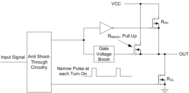
The UCC27517A is capable of delivering 4-A source, 4-A sink (symmetrical drive) at VDD = 12 V. The output stage of the UCC27517A device is illustrated in Figure 21. The UCC27517A features a unique architecture on the output stage which delivers the highest peak-source current when most needed during the Miller-plateau region of the power-switch turnon transition (when the power-switch drain/collector voltage experiences dV/dt). The device output stage features a hybrid pullup structure using a parallel arrangement of N-Channel and P-Channel MOSFET devices. By turning on the N-Channel MOSFET during a narrow instant when the output changes state from low to high, the gate-driver device delivers a brief boost in the peak-sourcing current enabling fast turnon.
 Figure 21. UCC27517A Gate Driver Output Structure
The ROH parameter (see Electrical Characteristics) is a DC measurement and is representative of the on-resistance of the P-Channel device only, since the N-Channel device is turned on only during output change of state from low to high. Thus the effective resistance of the hybrid pullup stage is much lower than what is represented by ROH parameter. The pulldown structure is composed of a N-Channel MOSFET only. The ROL parameter (see Electrical Characteristics), which is also a DC measurement, is representative of true impedance of the pulldown stage in the device. In the UCC27517A, the effective resistance of the hybrid pullup structure is approximately 1.4 × ROL.
The driver-output voltage swings between VDD and GND providing rail-to-rail operation because of the MOS output stage which delivers very low dropout. The presence of the MOSFET-body diodes also offers low impedance to switching overshoots and undershoots. This means that in many cases, external Schottky-diode clamps may be eliminated. The outputs of these drivers are designed to withstand 500-mA reverse current without either damage to the device or logic malfunction.
9.3.6 Low Propagation Delays
The UCC27517A features best-in-class input-to-output propagation delay of 13 ns (typ) at VDD = 12 V. This promises the lowest level of pulse-transmission distortion available from industry-standard gate-driver devices for high-frequency switching applications. As seen in Figure 14, there is very little variation of the propagation delay with temperature and supply voltage as well, offering typically less than 20-ns propagation delays across the entire range of application conditions.
9.4 Device Functional Modes
The device operates in normal mode and UVLO mode. See the VDD and Undervoltage Lockout section for information on UVLO operation mode. In the normal mode the output state is dependent on states of the IN+ and IN– pins. Table 4 below lists the output states for different input pin combinations.