ZHCSIB2B December 2017 – October 2019 UCC28064A
PRODUCTION DATA.
- 1 特性
- 2 应用
- 3 说明
- 4 修订历史记录
- 5 说明 (续)
- 6 Pin Configuration and Functions
- 7 Specifications
-
8 Detailed Description
- 8.1 Overview
- 8.2 Functional Block Diagram
- 8.3
Feature Description
- 8.3.1 Principles of Operation
- 8.3.2 Natural Interleaving
- 8.3.3 On-Time Control, Maximum Frequency Limiting, Restart Timer and Input Voltage Feed-Forward compensation
- 8.3.4 Distortion Reduction
- 8.3.5 Zero-Current Detection and Valley Switching
- 8.3.6 Phase Management and Light-Load Operation
- 8.3.7 Burst Mode Operation
- 8.3.8 External Disable
- 8.3.9 Improved Error Amplifier
- 8.3.10 Soft Start
- 8.3.11 Brownout Protection
- 8.3.12 Line Dropout Detection
- 8.3.13 VREF
- 8.3.14 VCC
- 8.3.15
System Level Protections
- 8.3.15.1 Failsafe OVP - Output Over-voltage Protection
- 8.3.15.2 Overcurrent Protection
- 8.3.15.3 Open-Loop Protection
- 8.3.15.4 VCC Undervoltage Lock-Out (UVLO) Protection
- 8.3.15.5 Phase-Fail Protection
- 8.3.15.6 CS - Open, TSET - Open and Short Protection
- 8.3.15.7 Thermal Shutdown Protection
- 8.3.15.8 Fault Logic Diagram
- 8.4 Device Functional Modes
-
9 Application and Implementation
- 9.1 Application Information
- 9.2
Typical Application
- 9.2.1 Design Requirements
- 9.2.2
Detailed Design Procedure
- 9.2.2.1 Custom Design With WEBENCH® Tools
- 9.2.2.2 Inductor Selection
- 9.2.2.3 ZCD Resistor Selection RZA, RZB
- 9.2.2.4 HVSEN
- 9.2.2.5 Output Capacitor Selection
- 9.2.2.6 Selecting RS For Peak Current Limiting
- 9.2.2.7 Power Semiconductor Selection (Q1, Q2, D1, D2)
- 9.2.2.8 Brownout Protection
- 9.2.2.9 Converter Timing
- 9.2.2.10 Programming VOUT
- 9.2.2.11 Voltage Loop Compensation
- 9.2.3 Application Curves
- 10Power Supply Recommendations
- 11Layout
- 12Package Option Addendum
- 13器件和文档支持
- 14机械、封装和可订购信息
8.3.4 Distortion Reduction
Due to the parasitic resonance between the drain-source capacitance of the switching MOSFET and the boost inductor, conventional transition-mode PFC circuits may not be able to absorb power from the input line when the input voltage is near zero. This limitation increases total harmonic distortion as a result of ac-line current waveform distortion in the form of flat spots. To help reduce line-current distortion, the UCC28064A increases switching MOSFET on-time when the input voltage is near 0 V to improve the power absorption capability and compensate for this effect.
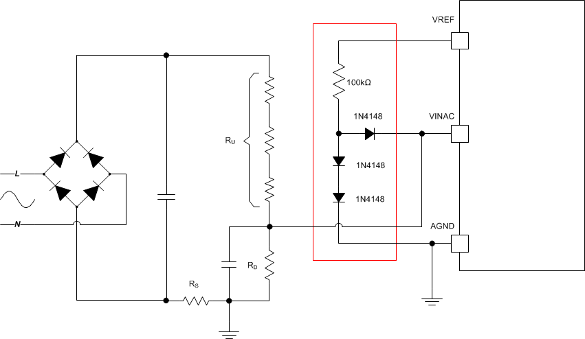
Figure 1 in the Typical Characteristics section shows the increase in on-time with respect to VINAC voltage. Excessive filtering of the VINAC signal will nullify this function. In cases where small inductances are used (< 250 µH) the increased MOSFET on time can be excessive, increasing distortion instead of decreasing. If this is the case the external circuit shown in Figure 17 can help limit this effect.
 Figure 17. External Circuit to improve THD in case of Low inductance