SLUSA29D April 2010 – August 2015 UCC28250
PRODUCTION DATA.
- 1 Features
- 2 Applications
- 3 Description
- 4 Revision History
- 5 Pin Configuration and Functions
- 6 Specifications
-
7 Detailed Description
- 7.1 Overview
- 7.2 Functional Block Diagram
- 7.3
Feature Description
- 7.3.1 VDD (5/12)
- 7.3.2 VREF (Reference Generator) (20/7)
- 7.3.3 EN (Enable Pin) (18/5)
- 7.3.4 RT (Oscillator Frequency Set and Synchronization) (15/2)
- 7.3.5 SP (Synchronous Rectifier Turnoff to Primary Output Turnon Dead Time Programming) (13/19)
- 7.3.6 PS (Primary Output Turnoff to Synchronous Rectifier Turnon Dead Time Programming) (11/18)
- 7.3.7 RAMP/CS (PWM Ramp Input or Current Sense Input) (16/3)
- 7.3.8 REF/EA+ (1/8)
- 7.3.9 FB/EA- (2/9)
- 7.3.10 COMP (3/10)
- 7.3.11 VSENSE (14/1)
- 7.3.12 SS (Soft Start Programming Pin) (13/20)
- 7.3.13 ILIM (Current Limit for Cycle-By-Cycle Overcurrent Protection) (17/4)
- 7.3.14 HICC (10/17)
- 7.3.15 OVP/OTP (19/6)
- 7.3.16 OUTA (9/16) and OUTB (8/15)
- 7.3.17 SRA (7/14) and SRB (6/13)
- 7.3.18 GND (4/11)
- 7.4 Device Functional Modes
-
8 Applications and Implementation
- 8.1 Application Information
- 8.2
Typical Applications
- 8.2.1
Design Example
- 8.2.1.1 Design Requirements
- 8.2.1.2
Detailed Design Procedure
- 8.2.1.2.1 Step 1, Power Stage Design
- 8.2.1.2.2 Step 2, Feedback Loop Design
- 8.2.1.2.3 Step 3, Programming the Device
- 8.2.1.2.4 Step 3-3, Determine Soft-Start Capacitance
- 8.2.1.2.5 Step 3-4, Determine Dead-Time Resistance
- 8.2.1.2.6 Step 3-5, Determine OCP Hiccup Off-Time Capacitance
- 8.2.1.2.7 Step 3-6, Determine Primary-Side OVP Resistance
- 8.2.1.2.8 Step 3-7, Select Capacitance for VDD and VREF
- 8.2.1.3 Application Curves
- 8.2.2 Secondary-Side Half-Bridge Controller with Synchronous Rectification
- 8.2.1
Design Example
- 9 Power Supply Recommendations
- 10Layout
- 11Device and Documentation Support
- 12Mechanical, Packaging, and Orderable Information
封装选项
机械数据 (封装 | 引脚)
散热焊盘机械数据 (封装 | 引脚)
- RGP|20
订购信息
6 Specifications
6.1 Absolute Maximum Ratings
over operating free-air temperature range(1)(2) (unless otherwise noted)| MIN | MAX | UNIT | ||
|---|---|---|---|---|
| VDD(3) | Input supply voltage | –0.3 | 20 | V |
| OUTA, OUTB, SRA and SRB | –0.3 | VDD + 0.3 | V | |
| COMP | –0.3 | VREF + 0.3 | V | |
| Input voltages on SS and EN | –0.3 | 5.5 | V | |
| Input voltages on RT, PS, SP, ILIM, OVP, HICC, VSENSE, EA+ and EA- | –0.3 | 3.6 | V | |
| Input voltage on RAMP/CS | –0.3 | 4.3 | V | |
| Output voltage on VREF | –0.3 | 3.6 | V | |
| Lead temperature (soldering 10 sec) PW package | 300 | °C | ||
| Tstg | Storage temperature | –65 | 150 | °C |
(1) Stresses beyond those listed under Absolute Maximum Ratings may cause permanent damage to the device. These are stress ratings only, which do not imply functional operation of the device at these or any other conditions beyond those indicated under Recommended Operating Conditions. Exposure to absolute-maximum-rated conditions for extended periods may affect device reliability.
(2) These devices are sensitive to electrostatic discharge; follow proper device handling procedures.
(3) All voltages are with respect to GND unless otherwise noted. Currents are positive into, negative out of the specified terminal. See Mechanical, Packaging, and Orderable Information of the data sheet for thermal limitations and considerations of packages.
6.2 ESD Ratings
| VALUE | UNIT | |||
|---|---|---|---|---|
| V(ESD) | Electrostatic discharge | Human-body model (HBM), per ANSI/ESDA/JEDEC JS-001(1) | ±3000 | V |
| Charged-device model (CDM), per JEDEC specification JESD22-C101(2) | ±2000 | |||
(1) JEDEC document JEP155 states that 500-V HBM allows safe manufacturing with a standard ESD control process.
(2) JEDEC document JEP157 states that 250-V CDM allows safe manufacturing with a standard ESD control process.
6.3 Recommended Operating Conditions
over operating free-air temperature range (unless otherwise noted)6.4 Thermal Information
| THERMAL METRIC | UCC28250 | UNIT | ||
|---|---|---|---|---|
| RGB (VQFN) | PW (TSSOP) | |||
| 20 PINS | 20 PINS | |||
| RθJA | Junction-to-ambient thermal resistance | 126 with hot spot, 104 without hot spot |
60.3 with hot spot, 39.3 without hot spot |
°C/W |
| RθJC(top) | Junction-to-case(top) thermal resistance | 31.5 | °C/W | |
| RθJB | Junction-to-board thermal resistance | 55.8 | °C/W | |
| RθJC(bot) | Junction-to-case(bottom) thermal resistance | 0.8 | °C/W | |
6.5 Electrical Characteristics
VDD = 12 V, 1-µF capacitor from VDD and VREF to GND, TA = TJ = –40°C to 125°C, RT = 75 kΩ connected to ground to set FSW = 200 kHz (unless otherwise noted). (1)| PARAMETER | TEST CONDITIONS | MIN | TYP | MAX | UNIT | |
|---|---|---|---|---|---|---|
| SUPPLY CURRENTS | ||||||
| IDD(off) | Start-up current | VDD = 3.6 V | 150 | 275 | µA | |
| IDD | Operating supply current | 100-pF capacitor on OUTA, OUTB, SRA and SRB | 2 | 2.7 | 3.4 | mA |
| IDD(dis) | Standby current | EN = 0 V | 250 | 425 | 600 | µA |
| UNDERVOLTAGE LOCKOUT | ||||||
| VUVLOR | Start threshold | 4 | 4.3 | 4.6 | V | |
| VUVLOF | Minimum operating voltage after start | 3.8 | 4.1 | 4.4 | V | |
| Hysteresis | 0.15 | 0.2 | 0.25 | V | ||
| SOFT START | ||||||
| ISS | Soft-start charge current | VSS = 0 V | 25 | 27 | 29 | µA |
| VSS(max) | Clamp voltage | 3.3 | 3.6 | 4 | V | |
| ENABLE(2) | ||||||
| Trigger threshold | 2.25 | V | ||||
| Minimum pulse width for pulse enable | 3 | µs | ||||
| ERROR AMPLIFIER | ||||||
| High-level COMP voltage | 2.8 | 3 | V | |||
| Low-level COMP voltage | 0.3 | 0.4 | V | |||
| Input offset | -12 | 12 | mV | |||
| Open loop gain | 70 | 100 | dB | |||
| ICOMP(snk) | COMP sink current | 3 | 6.5 | 9 | mA | |
| ICOMP(src) | COMP source current | 2 | 4.5 | 8 | mA | |
| OSCILLATOR | ||||||
| FSW(nom) | Nominal switching frequency at OUTA or OUTB set by RT resistor | RT/SYNC = 75 kΩ, RSP = 20 kΩ | 185 | 200 | 215 | kHz |
| FSW(min_sync) | Minimum switching frequency at OUTA or OUTB set by external sync frequency | fRT/SYNC = 100 kHz | 85 | kHz | ||
| FSW(max_sync) | Maximum switching frequency at OUTA or OUTB set by external sync frequency | fRT/SYNC = 2.5 MHz | 1.15 | MHz | ||
| External synchronization signal high | 1 | V | ||||
| External synchronization signal low | 0.2 | V | ||||
| VOLTAGE REFERENCE | ||||||
| VVREF | Output voltage | VDD = from 7 V to 17 V, IVREF = 2 mA | 3.22 | 3.3 | 3.38 | V |
| 0 < IREF < 10 mA | 3.22 | 3.3 | 3.38 | |||
| Short circuit current | VREF = 3 V, TJ = 25°C | 12 | 25 | 40 | mA | |
| CURRENT SENSE, CYCLE-BY-CYCLE CURRENT LIMIT WITH HICCUP | ||||||
| VILIM | ILIM cycle-by-cycle threshold | 0.495 | 0.502 | 0.509 | V | |
| TPDILIM | Propagation delay from ILIM to OUTA and OUTB outputs | Exclude leading edge blanking | 15 | 25 | 36 | ns |
| TBLANK | leading edge blanking | 40 | 60 | 90 | ns | |
| Current limit shutdown delay timing program current | Measured at HICC pin | 55 | 75 | 95 | µA | |
| Hiccup timing program current | Measured at HICC pin | 2 | 2.7 | 3.5 | µA | |
| VHICC_SD | Current limit shutdown delay timer threshold at HICC | 0.55 | 0.6 | 0.65 | V | |
| VHICC_PU | HICC pullup threshold | 2.3 | 2.4 | 2.5 | V | |
| VHICC_RST | Hiccup restart threshold | 0.25 | 0.3 | 0.35 | V | |
| VCS(max) | RAMP/CS clamp voltage | 10-V ramp charging voltage source with 40-kΩ current limiting resistor | 3.5 | 4 | 4.5 | V |
| OVP/OTP COMPARATOR | ||||||
| VOVP | Internal reference | 0.66 | 0.7 | 0.74 | V | |
| IOVP | Internal current | 8.5 | 11 | 13.5 | µA | |
| PRIMARY OUTPUTS | ||||||
| Rise/fall time | CLOAD = 100 pF | 8 | ns | |||
| RSRC | Output source resistance | IOUT = 20 mA | 12 | 20 | 35 | Ω |
| RSNK | Output sink resistance | IOUT = 20 mA | 4 | 12 | 30 | Ω |
| SYNCHRONOUS RECTIFIER OUTPUTS | ||||||
| Rise/fall time | CLOAD = 100 pF | 8 | ns | |||
| RSRC | Output source resistance | IOUT = 20 mA, VDD = 12 V | 12 | 20 | 35 | Ω |
| IOUT = 20 mA, VDD = 5 V | 15 | 25 | 45 | |||
| RSNK | Output sink resistance | IOUT = 20 mA, VDD = 12 V | 4 | 12 | 30 | Ω |
| TDPS | Primary off to secondary on dead time | PS = VREF | -5 | 0 | 7.5 | ns |
| PS = 27 kΩ | 27 | 40 | 50 | |||
| PS = 27 kΩ, 25°C | 37 | 40 | 43 | |||
| TDSP | Secondary off to primary on dead time | SP = VREF | -5 | 0 | 7.5 | ns |
| SP = 20 kΩ | 30 | 40 | 50 | |||
| SP = 20 kΩ, 25°C | 37 | 40 | 43 | |||
(1) Typical values for TA = 25°C.
6.6 Typical Characteristics
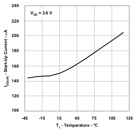 Figure 1. Start-up Current vs
 Temperature
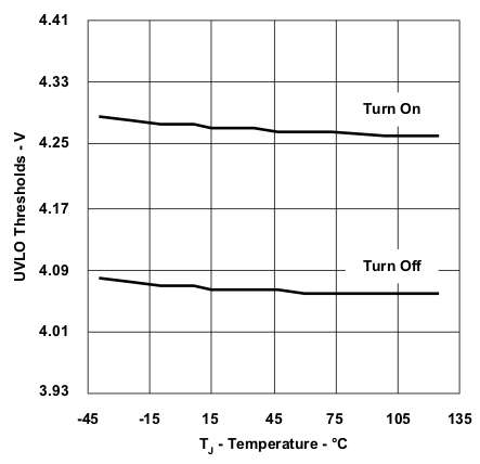 Figure 3. UVLO Thresholds vs
 Temperature
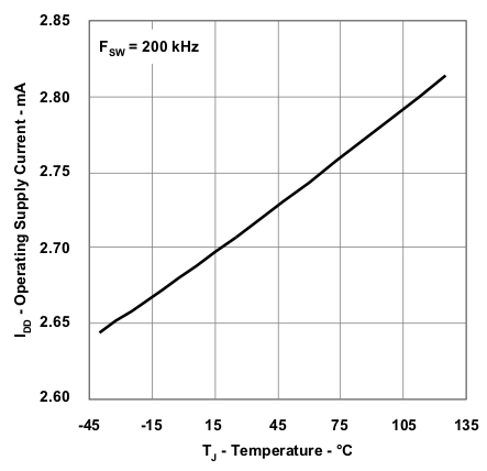 Figure 5. Operating Supply Current vs
Temperature
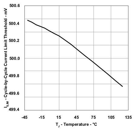 Figure 7. Cycle-by-Cycle Current Limit vs Temperature
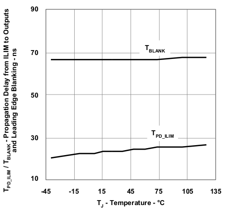 Figure 9. Propagation Delay and Leading Edge Blanking vs Temperature
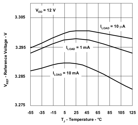 Figure 11. Reference Voltage vs Temperature
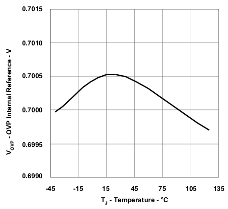 Figure 13. OVP Internal Reference vs Temperature
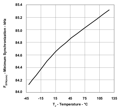 Figure 15. Minimum Synchronization Frequency vs Temperature
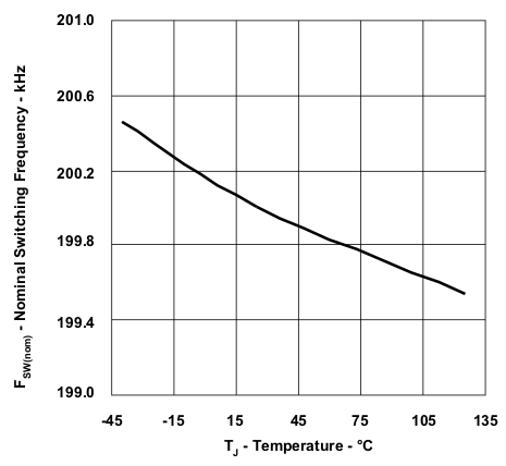 Figure 17. Nominal Switching Frequency vs Temperature
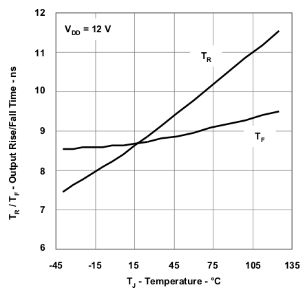 Figure 19. Output Rise/Fall Time vs Temperature
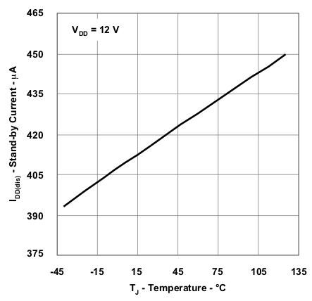 Figure 2. Stand-by Current vs Temperature
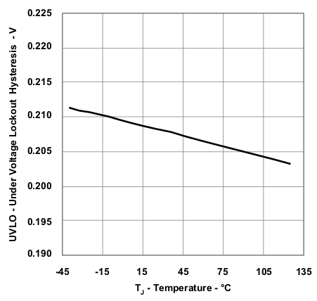 Figure 4. UVLO Voltage Lockout Hysteresis
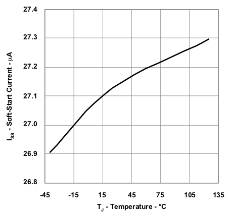 Figure 6. Soft-start Current vs Temperature
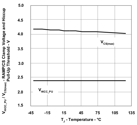 Figure 8. RAMP/CS Clamp Voltage and Hiccup Pullup Threshold vs Temperature
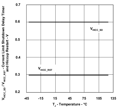 Figure 10. Current Limit Shutdown Delay Timer and Hiccup Restart vs Temperature
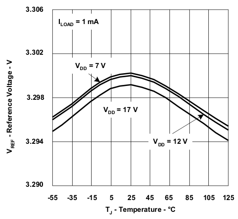 Figure 12. Reference Voltage vs Temperature
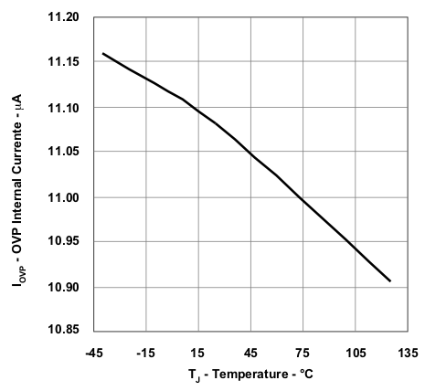 Figure 14. OVP Internal Current vs Temperature
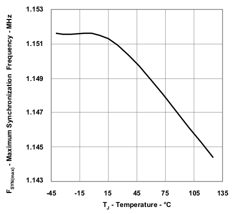 Figure 16. Maximum Synchronization Frequency vs Temperature
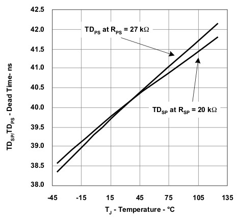 Figure 18. Dead Time vs Temperature
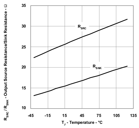 Figure 20. Output Source Resistance/Sink Resistance vs Temperature