ZHCSK44G December 2009 – November 2022 UCC28C40-Q1 , UCC28C41-Q1 , UCC28C42-Q1 , UCC28C43-Q1 , UCC28C44-Q1 , UCC28C45-Q1
PRODUCTION DATA
- 1 特性
- 2 应用
- 3 说明
- 4 Revision History
- 5 Device Comparison Table
- 6 Pin Configuration and Functions
- 7 Specifications
-
8 Detailed Description
- 8.1 Overview
- 8.2 Functional Block Diagram
- 8.3 Feature Description
- 8.4 Device Functional Modes
-
9 Application and Implementation
- 9.1 Application Information
- 9.2
Typical Application
- 9.2.1 Design Requirements
- 9.2.2
Detailed Design Procedure
- 9.2.2.1 Custom Design With WEBENCH® Tools
- 9.2.2.2 Input Bulk Capacitor and Minimum Bulk Voltage
- 9.2.2.3 Transformer Turns Ratio and Maximum Duty CycleG
- 9.2.2.4 Transformer Inductance and Peak Currents
- 9.2.2.5 Output Capacitor
- 9.2.2.6 Current Sensing Network
- 9.2.2.7 Gate Drive Resistor
- 9.2.2.8 VREF Capacitor
- 9.2.2.9 RT/CT
- 9.2.2.10 Start-Up Circuit
- 9.2.2.11 Voltage Feedback Compensation
- 9.2.3 Application Curves
- 9.2.4 Power Supply Recommendations
- 9.2.5 Layout
- 10Device and Documentation Support
- 11Mechanical, Packaging, and Orderable Information
8.3.1.7 VDD
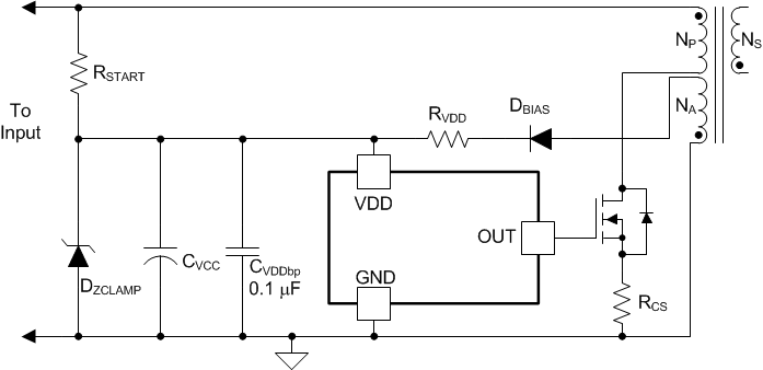
VDD is the power input connection for this device. In normal operation, power VDD through a current limiting resistor. The absolute maximum supply voltage is 20 V, including any transients that may be present. If this voltage is exceeded, device damage is likely. This is in contrast to the predecessor bipolar devices, which could survive up to 30 V on the input bias pin. Also, because no internal clamp is included in the device, the VDD pin must be protected from external sources which could exceed the 20 V level. If containing the start-up and bootstrap supply voltage from the auxiliary winding NA below 20 V under all line and load conditions can not be achieved, use a zener protection diode from VDD to GND. Depending on the impedance and arrangement of the bootstrap supply, this may require adding a resistor, RVDD, in series with the auxiliary winding to limit the current into the zener as shown in Figure 8-1. Insure that over all tolerances and temperatures, the minimum zener voltage is higher than the highest UVLO upper turnon threshold. To ensure against noise related problems, filter VDD with a ceramic bypass capacitor to GND. The VDD pin must be decoupled as close to the GND pin as possible.
 Figure 8-1 VDD Protection
Although quiescent VDD current is only 2.3 mA, the total supply current is higher, depending on the OUT current. Total VDD current is the sum of quiescent VDD current and the average OUT current. Knowing the operating frequency and the MOSFET gate charge (Qg), average OUT current can be calculated from Equation 1.
