ZHCSQ75C June 2022 – March 2023 UCC28C50-Q1 , UCC28C51-Q1 , UCC28C52-Q1 , UCC28C53-Q1 , UCC28C54-Q1 , UCC28C55-Q1 , UCC28C56H-Q1 , UCC28C56L-Q1 , UCC28C57H-Q1 , UCC28C57L-Q1 , UCC28C58-Q1 , UCC28C59-Q1
PRODUCTION DATA
- 1 特性
- 2 应用
- 3 说明
- 4 Revision History
- 5 Device Comparison Table
- 6 Pin Configuration and Functions
- 7 Specifications
-
8 Detailed Description
- 8.1 Overview
- 8.2 Functional Block Diagram
- 8.3 Feature Description
- 8.4 Device Functional Modes
-
9 Application and Implementation
- 9.1 Application Information
- 9.2
Typical Application
- 9.2.1 Design Requirements
- 9.2.2
Detailed Design Procedure
- 9.2.2.1 Primary-to-Secondary Turns Ratio of the Flyback Transformer (NPS)
- 9.2.2.2 Primary Magnetizing Inductance of the Flyback Transformer (LM)
- 9.2.2.3 Number of Turns of the Flyback Transformer Windings
- 9.2.2.4 Current Sense Resistors (R24, R25) and Current Limiting
- 9.2.2.5 Primary Clamp Circuit (D7, D1, D3, R2, R28) to Limit Voltage Stress
- 9.2.2.6 Primary-Side Current Stress and Input Capacitor Selection
- 9.2.2.7 Secondary-Side Current Stress and Output Capacitor Selection
- 9.2.2.8 VDD Capacitors (C12, C18)
- 9.2.2.9 Gate Drive Network (R14, R16, Q6)
- 9.2.2.10 VREF Capacitor (C18)
- 9.2.2.11 RT/CT Components (R12, C15)
- 9.2.2.12 HV Start-Up Circuitry for VDD (Q1, Q2, D2, D4, D6, D8, R5)
- 9.2.2.13 Desensitization to CS-pin Noise by RC Filtering, Leading-Edge Blanking, and Slope Compensation
- 9.2.2.14 Voltage Feedback Compensation
- 9.2.3 Application Curves
- 9.3 PCB Layout Recommendations
- 9.4 Power Supply Recommendations
- 10Device and Documentation Support
- 11Mechanical, Packaging, and Orderable Information
8.3.8 Enable and Disable
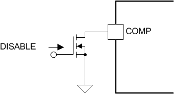
There are a few ways to enable or disable the UCC28C5x-Q1 devices, depending on which type of restart is required. The two basic techniques use external transistors to either pull the error amplifier output low (< 2 VBE) or pull the current sense input high (> 1.1 V). Application of the disable signal causes the output of the PWM comparator to be high. The PWM latch is reset dominant so that the output remains low until the next clock cycle after the shutdown condition at the COMP or CS pin is removed. Another choice for restart without a soft start is to pull the current sense input above the cycle-by-cycle current limiting threshold. A logic level P-channel FET from the reference voltage to the current sense input can be used.
 Figure 8-7 Disable Circuit