ZHCSQ75C June 2022 – March 2023 UCC28C50-Q1 , UCC28C51-Q1 , UCC28C52-Q1 , UCC28C53-Q1 , UCC28C54-Q1 , UCC28C55-Q1 , UCC28C56H-Q1 , UCC28C56L-Q1 , UCC28C57H-Q1 , UCC28C57L-Q1 , UCC28C58-Q1 , UCC28C59-Q1
PRODUCTION DATA
- 1 特性
- 2 应用
- 3 说明
- 4 Revision History
- 5 Device Comparison Table
- 6 Pin Configuration and Functions
- 7 Specifications
-
8 Detailed Description
- 8.1 Overview
- 8.2 Functional Block Diagram
- 8.3 Feature Description
- 8.4 Device Functional Modes
-
9 Application and Implementation
- 9.1 Application Information
- 9.2
Typical Application
- 9.2.1 Design Requirements
- 9.2.2
Detailed Design Procedure
- 9.2.2.1 Primary-to-Secondary Turns Ratio of the Flyback Transformer (NPS)
- 9.2.2.2 Primary Magnetizing Inductance of the Flyback Transformer (LM)
- 9.2.2.3 Number of Turns of the Flyback Transformer Windings
- 9.2.2.4 Current Sense Resistors (R24, R25) and Current Limiting
- 9.2.2.5 Primary Clamp Circuit (D7, D1, D3, R2, R28) to Limit Voltage Stress
- 9.2.2.6 Primary-Side Current Stress and Input Capacitor Selection
- 9.2.2.7 Secondary-Side Current Stress and Output Capacitor Selection
- 9.2.2.8 VDD Capacitors (C12, C18)
- 9.2.2.9 Gate Drive Network (R14, R16, Q6)
- 9.2.2.10 VREF Capacitor (C18)
- 9.2.2.11 RT/CT Components (R12, C15)
- 9.2.2.12 HV Start-Up Circuitry for VDD (Q1, Q2, D2, D4, D6, D8, R5)
- 9.2.2.13 Desensitization to CS-pin Noise by RC Filtering, Leading-Edge Blanking, and Slope Compensation
- 9.2.2.14 Voltage Feedback Compensation
- 9.2.3 Application Curves
- 9.3 PCB Layout Recommendations
- 9.4 Power Supply Recommendations
- 10Device and Documentation Support
- 11Mechanical, Packaging, and Orderable Information
9.2.3 Application Curves
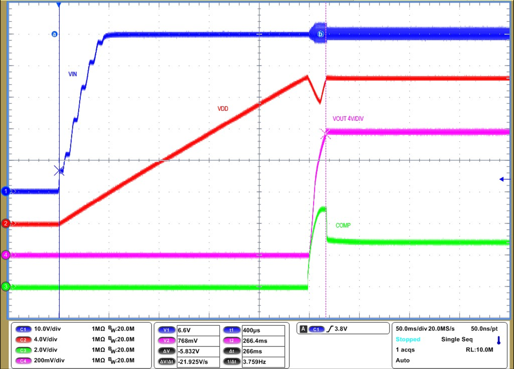
| VIN applied to VOUT ready in 266 ms |
| CH1: VIN at 10 V/DIV |
| CH2: VDD at 4 V/DIV |
| CH3: COMP at 2 V/DIV |
| CH4: VOUT at 4 V/DIV via differential probe |

| VDD capacitor hold-up time = 12.6 ms |
| VOUT rise time = 17.2 ms |
| CH2: VDD at 4 V/DIV |
| CH3: COMP at 2V/DIV |
| CH4: VOUT at 4 V/DIV via differential probe |
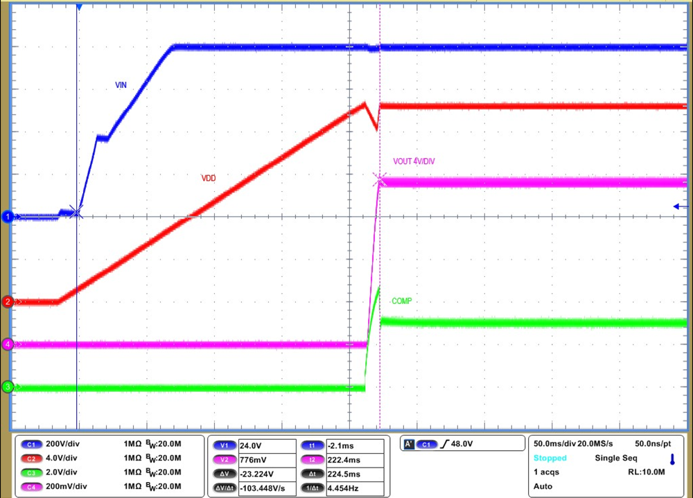
| VIN applied to VOUT ready in 224 ms |
| CH1: VIN at 200 V/DIV |
| CH2: VDD at 4 V/DIV |
| CH3: COMP at 2 V/DIV |
| CH4: VOUT at 4 V/DIV via differential probe |
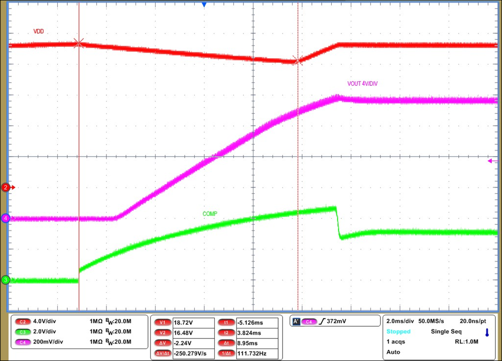
| VDD capacitor hold-up time = 8.9 ms |
| VOUT rise time = 9.1 ms |
| CH2: VDD at 4 V/DIV |
| CH3: COMP at 2V/DIV |
| CH4: VOUT at 4 V/DIV via differential probe |

| Soft Start Overshoot = 1.2 % |
| CH4: VOUT at 1 V/DIV via differential probe |
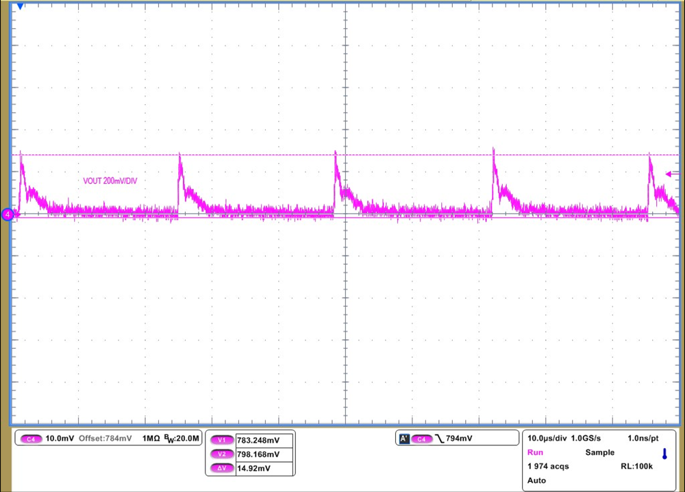
| Output Voltage Ripple = 298 mVPP |
| CH4: VOUT at 200 mV/DIV via differential probe |
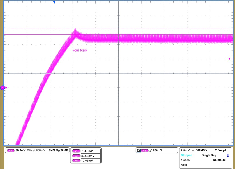
| Soft Start Overshoot = 2.4 % |
| CH4: VOUT at 1 V/DIV via differential probe |
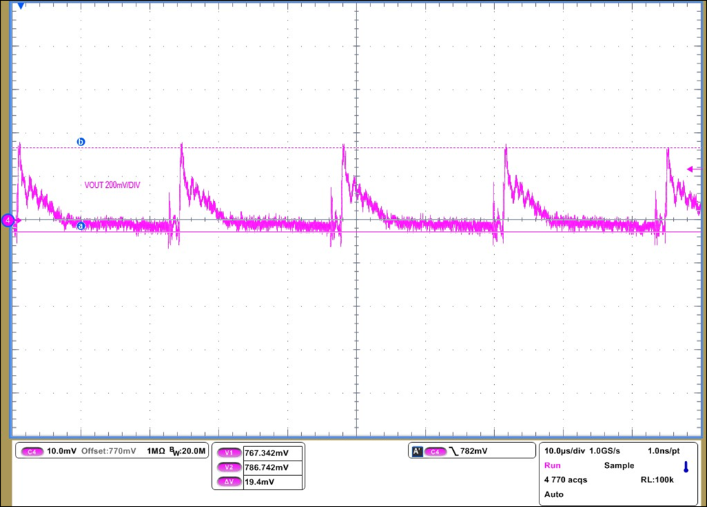
| Output Voltage Ripple = 388 mVPP |
| CH4: VOUT at 200 mV/DIV via differential probe |
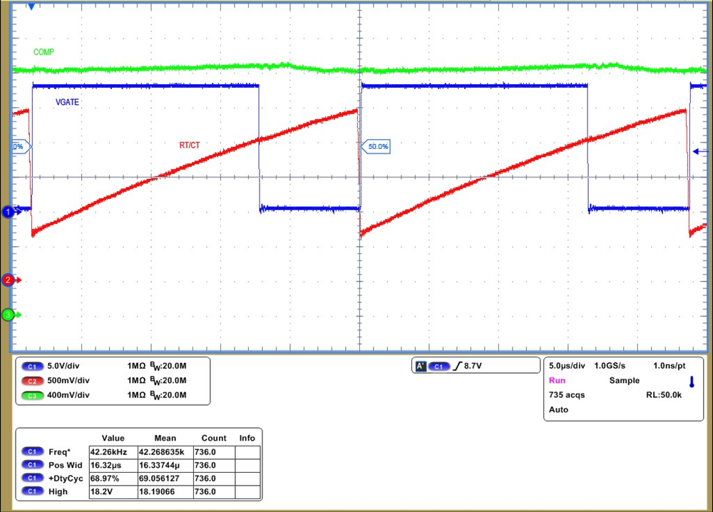
| fSW = 42.6 kHz, tON = 16.3 us, Duty Cycle = 69 % |
| CH1: VGATE at 5 V/DIV |
| CH2: RT/CT at 500 mV/DIV |
| CH3: COMP at 400 mV/DIV |

| 250 mA to 1.3 A to 250 mA |
| VMAX = 16.1 V, VMIN = 15.4 V, dV = 0.7 V |
| CH1: COMP at 50 mV/DIV |
| CH2: I_LOAD at 500 mA/DIV |
| CH4: VOUT at 600 mV/DIV via differential probe |
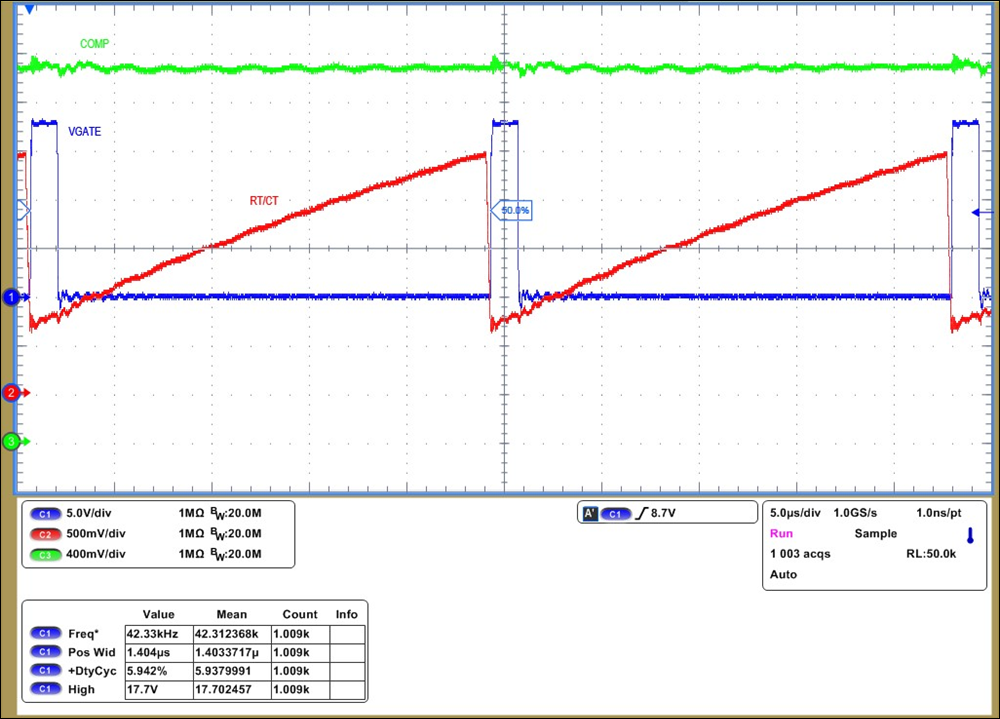
| fSW = 42.3 kHz, tON = 1.4 us, Duty Cycle = 5.9 % |
| CH1: VGATE at 5 V/DIV |
| CH2: RT/CT at 500 mV/DIV |
| CH3: COMP at 400 mV/DIV |
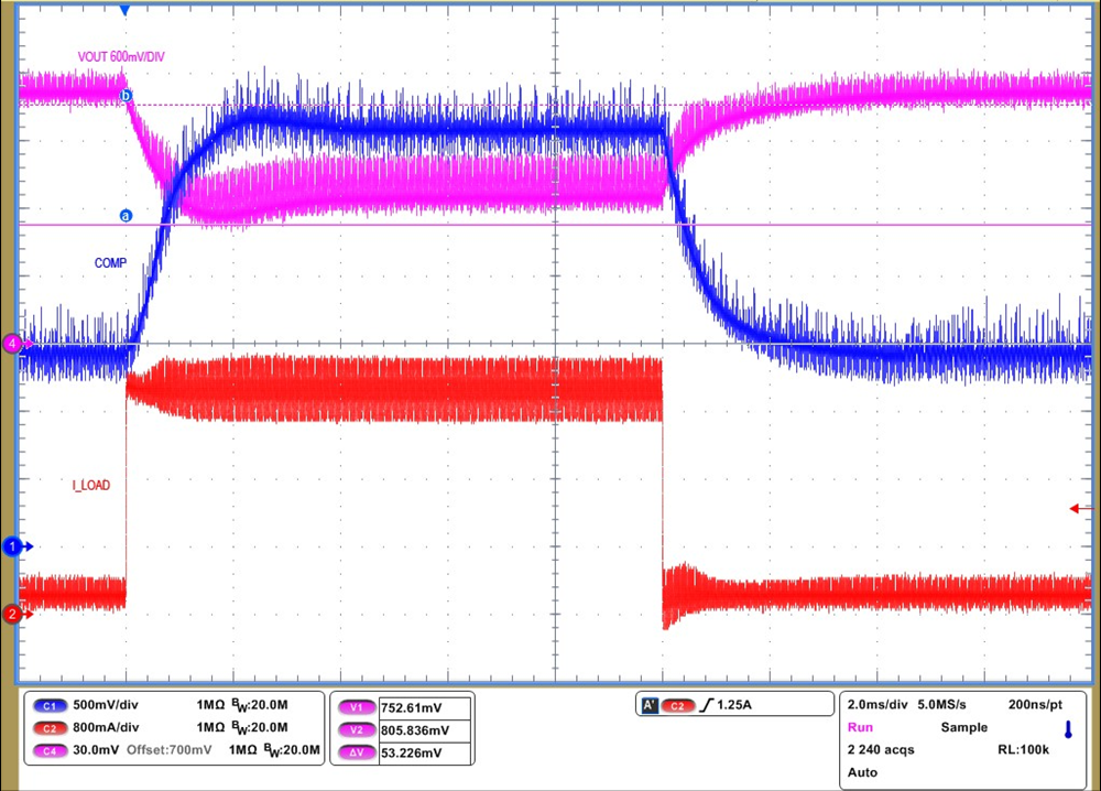
| 250 mA to 2.7 A to 250 mA |
| VMAX = 16.1 V, VMIN = 15.1V, dV = 1.0 V |
| CH1: COMP at 50 mV/DIV |
| CH2: I_LOAD at 800 mA/DIV |
| CH4: VOUT at 600 mV/DIV via differential probe |