ZHCSQ75C June 2022 – March 2023 UCC28C50-Q1 , UCC28C51-Q1 , UCC28C52-Q1 , UCC28C53-Q1 , UCC28C54-Q1 , UCC28C55-Q1 , UCC28C56H-Q1 , UCC28C56L-Q1 , UCC28C57H-Q1 , UCC28C57L-Q1 , UCC28C58-Q1 , UCC28C59-Q1
PRODUCTION DATA
- 1 特性
- 2 应用
- 3 说明
- 4 Revision History
- 5 Device Comparison Table
- 6 Pin Configuration and Functions
- 7 Specifications
-
8 Detailed Description
- 8.1 Overview
- 8.2 Functional Block Diagram
- 8.3 Feature Description
- 8.4 Device Functional Modes
-
9 Application and Implementation
- 9.1 Application Information
- 9.2
Typical Application
- 9.2.1 Design Requirements
- 9.2.2
Detailed Design Procedure
- 9.2.2.1 Primary-to-Secondary Turns Ratio of the Flyback Transformer (NPS)
- 9.2.2.2 Primary Magnetizing Inductance of the Flyback Transformer (LM)
- 9.2.2.3 Number of Turns of the Flyback Transformer Windings
- 9.2.2.4 Current Sense Resistors (R24, R25) and Current Limiting
- 9.2.2.5 Primary Clamp Circuit (D7, D1, D3, R2, R28) to Limit Voltage Stress
- 9.2.2.6 Primary-Side Current Stress and Input Capacitor Selection
- 9.2.2.7 Secondary-Side Current Stress and Output Capacitor Selection
- 9.2.2.8 VDD Capacitors (C12, C18)
- 9.2.2.9 Gate Drive Network (R14, R16, Q6)
- 9.2.2.10 VREF Capacitor (C18)
- 9.2.2.11 RT/CT Components (R12, C15)
- 9.2.2.12 HV Start-Up Circuitry for VDD (Q1, Q2, D2, D4, D6, D8, R5)
- 9.2.2.13 Desensitization to CS-pin Noise by RC Filtering, Leading-Edge Blanking, and Slope Compensation
- 9.2.2.14 Voltage Feedback Compensation
- 9.2.3 Application Curves
- 9.3 PCB Layout Recommendations
- 9.4 Power Supply Recommendations
- 10Device and Documentation Support
- 11Mechanical, Packaging, and Orderable Information
8.3.10 Voltage Mode
In certain applications, voltage mode control may be a preferred control strategy for a variety of reasons. Voltage mode control is easily executable with any current mode controller, especially the UCC28C5x-Q1 family members. Implementation requires generating a 0-V to 0.9-V sawtooth shaped signal to input to the current sense pin (CS) which is also one input to the PWM comparator. This is compared to the divided down error amplifier output voltage at the other input of the PWM comparator. As the error amplifier output is varied, it intersects the sawtooth waveform at different points in time, thereby generating different pulse widths. This is a straightforward method of linearly generating a pulse whose width is proportional to the error voltage.
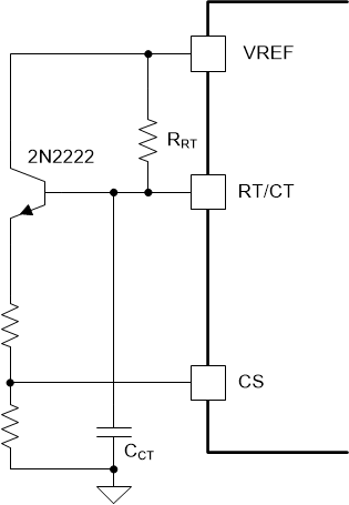
Implementation of voltage mode control is possible by using a fraction of the oscillator timing capacitor (CCT) waveform. This can be divided down and fed to the current sense pin as shown in Figure 8-9. The oscillator timing components must be selected to approximate as close to a linear sawtooth waveform as possible. Although exponentially charged, large values of timing resistance and small values of timing capacitance help approximate a more linear shaped waveform. A small transistor is used to buffer the oscillator timing components from the loading of the resistive divider network.
 Figure 8-9 Current Mode PWM Used as a
Voltage Mode PWM