ZHCSQ75C June 2022 – March 2023 UCC28C50-Q1 , UCC28C51-Q1 , UCC28C52-Q1 , UCC28C53-Q1 , UCC28C54-Q1 , UCC28C55-Q1 , UCC28C56H-Q1 , UCC28C56L-Q1 , UCC28C57H-Q1 , UCC28C57L-Q1 , UCC28C58-Q1 , UCC28C59-Q1
PRODUCTION DATA
- 1 特性
- 2 应用
- 3 说明
- 4 Revision History
- 5 Device Comparison Table
- 6 Pin Configuration and Functions
- 7 Specifications
-
8 Detailed Description
- 8.1 Overview
- 8.2 Functional Block Diagram
- 8.3 Feature Description
- 8.4 Device Functional Modes
-
9 Application and Implementation
- 9.1 Application Information
- 9.2
Typical Application
- 9.2.1 Design Requirements
- 9.2.2
Detailed Design Procedure
- 9.2.2.1 Primary-to-Secondary Turns Ratio of the Flyback Transformer (NPS)
- 9.2.2.2 Primary Magnetizing Inductance of the Flyback Transformer (LM)
- 9.2.2.3 Number of Turns of the Flyback Transformer Windings
- 9.2.2.4 Current Sense Resistors (R24, R25) and Current Limiting
- 9.2.2.5 Primary Clamp Circuit (D7, D1, D3, R2, R28) to Limit Voltage Stress
- 9.2.2.6 Primary-Side Current Stress and Input Capacitor Selection
- 9.2.2.7 Secondary-Side Current Stress and Output Capacitor Selection
- 9.2.2.8 VDD Capacitors (C12, C18)
- 9.2.2.9 Gate Drive Network (R14, R16, Q6)
- 9.2.2.10 VREF Capacitor (C18)
- 9.2.2.11 RT/CT Components (R12, C15)
- 9.2.2.12 HV Start-Up Circuitry for VDD (Q1, Q2, D2, D4, D6, D8, R5)
- 9.2.2.13 Desensitization to CS-pin Noise by RC Filtering, Leading-Edge Blanking, and Slope Compensation
- 9.2.2.14 Voltage Feedback Compensation
- 9.2.3 Application Curves
- 9.3 PCB Layout Recommendations
- 9.4 Power Supply Recommendations
- 10Device and Documentation Support
- 11Mechanical, Packaging, and Orderable Information
9.3.1 PCB Layout Routing Examples
1) The power ground should not disturb (i.e. mix with) the signal ground. The signal ground includes the small R’s and C’s around the controller (for COMP, FB, RT/CT, CS) and the controller ground pin. The power ground includes the input capacitors, current sense resistors, return for the Y-capacitor, and gate drive return via the PNP transistor Q6.
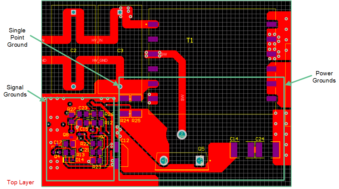 Figure 9-22 Top
Layer: Signal Grounds, Power Grounds, and their Connection to a Single-Point
Ground
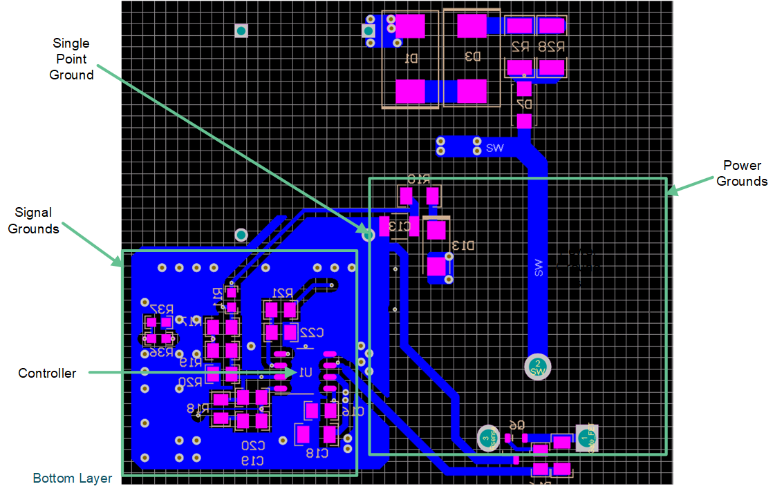 Figure 9-23 Bottom
Layer: Signal Grounds, Power Grounds, and their Connection to a Single-Point
Ground
Figure 9-23 Bottom
Layer: Signal Grounds, Power Grounds, and their Connection to a Single-Point
Ground2) The primary-side power loop must be minimized. Use relatively wide traces. This loop includes the input capacitors (C2, C3), transformer primary winding (T1 pins 1, 3), switching MOSFET (Q5), and sense resistors (R24, R25). Do not use vias in this path.
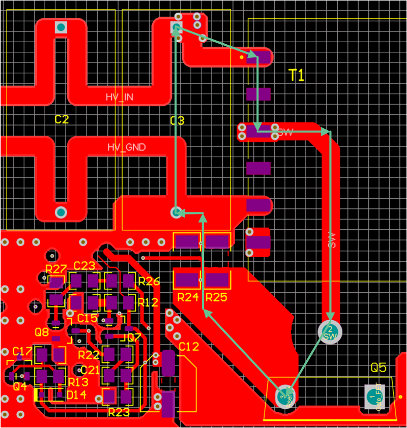 Figure 9-24 Primary-Side Power Loop Routing
3) The secondary-side power loop should be minimized. Use copper pours or very wide traces. This loop includes the output capacitors (C9, C10), transformer secondary winding (T1 pins 8/9, 10/11), and output rectifier diode (D11). If interconnection between layers is required use multiple vias to handle the high peak currents.
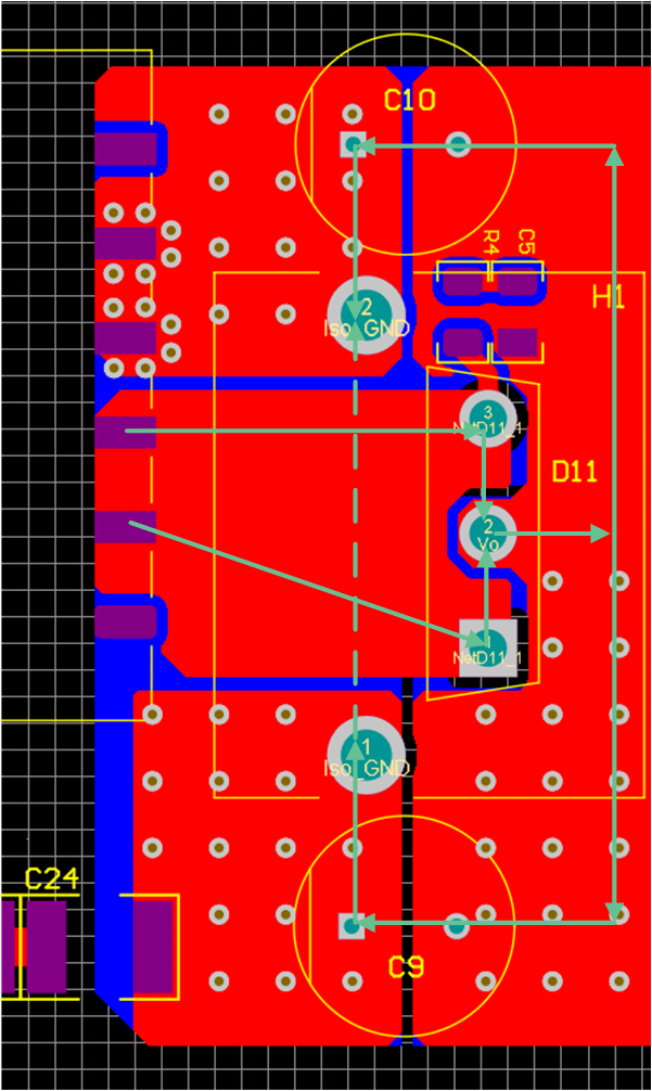 Figure 9-25 Secondary-Side Power Loop Routing
4) The AUX feedback loop should be minimized. This loop includes components C13, D13, and the transformer AUX winding (T1 pins 6, 5).
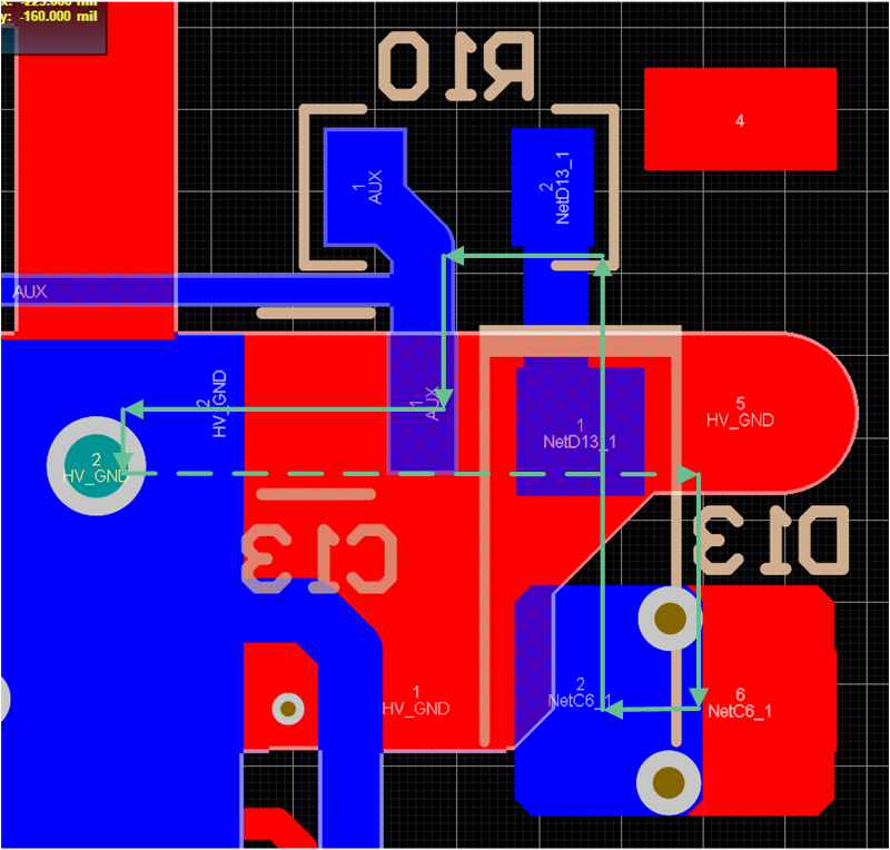 Figure 9-26 AUX
Feedback Loop Routing
Figure 9-26 AUX
Feedback Loop Routing5) The loop of the high-voltage clamp must be minimized. This loop includes D1, D3, R2//R28, and D7. All these components should be on the same layer.
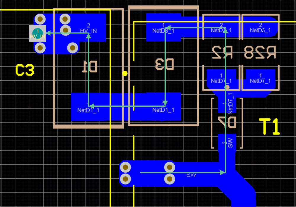 Figure 9-27 High-Voltage Clamp Loop Routing
6) The Y-type capacitor from the isolation ground to the power ground (C14, C24) should route back to the single point ground without disturbing the signal ground around the controller.
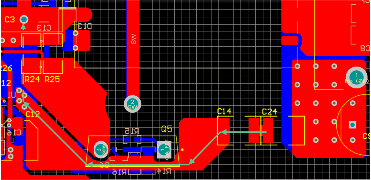 Figure 9-28 Y-Capacitor Ground Routing
7) The trace from the OUT pin (U1 pin 6) to the gate of the switching MOSFET (Q5-1) must be as short as possible and relatively wide. Do not use vias in this path.
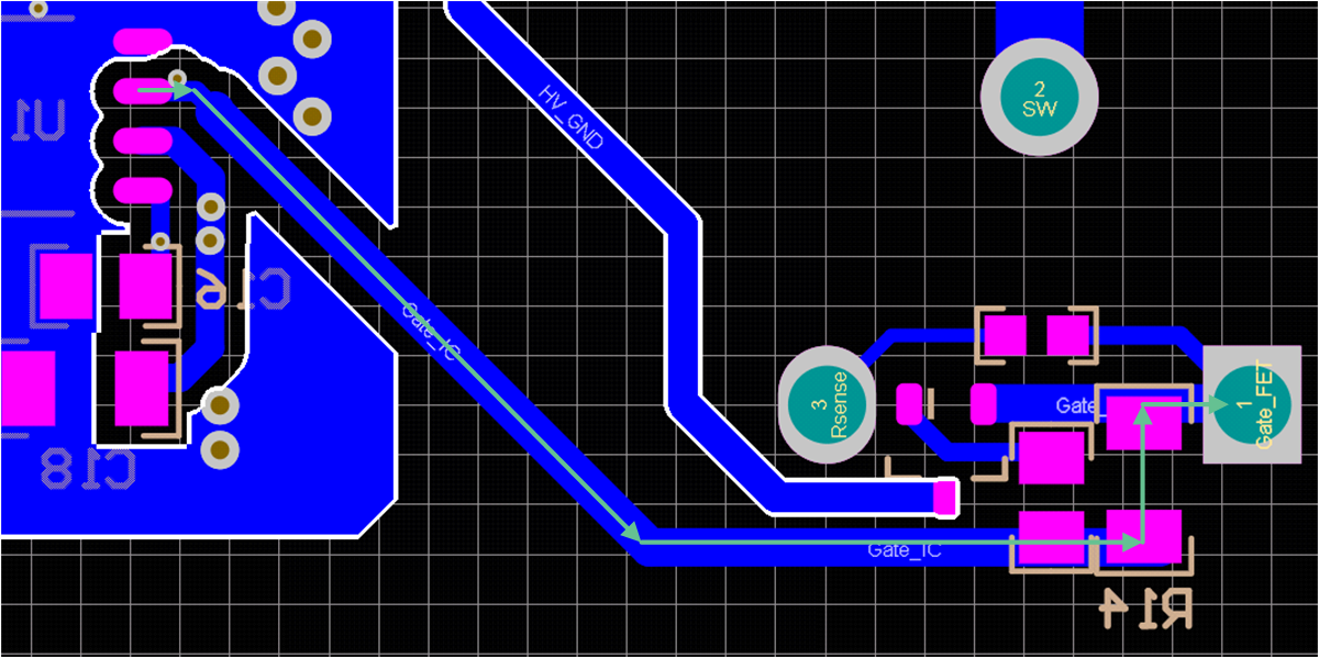 Figure 9-29 Gate
Drive (OUT) Trace Routing
Figure 9-29 Gate
Drive (OUT) Trace Routing8) The collector of the PNP gate pull-down transistor (Q6 pin 3) should route directly back to the single point ground without disturbing the signal ground around the controller.
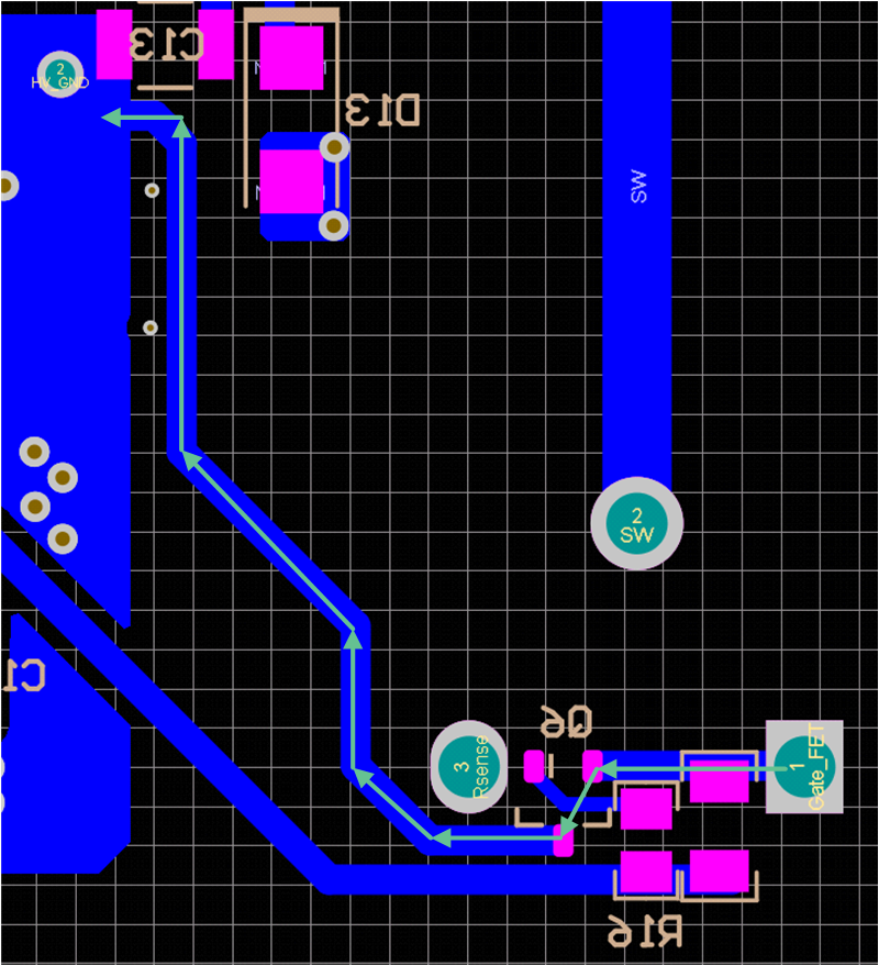 Figure 9-30 Gate
Pull-Down PNP Transistor Collector Routing
Figure 9-30 Gate
Pull-Down PNP Transistor Collector Routing9) The connection from the current sense resistors (R24/R25) to the low-pass filter (R21, C22) and on to the CS pin must be direct and it must avoid noisy signals. For example, do not route this trace near the MOSFET gate drive or SW node.
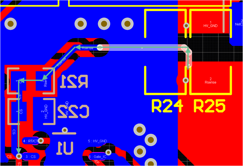 Figure 9-31 Current
Sense Trace Routing
Figure 9-31 Current
Sense Trace Routing10) The loop formed by the R-C snubber (R4, C5) around the output rectifier diode (D11) should be minimized. Do not use vias in this path.
11) The VDD pin must have a ceramic capacitor (C18) located as close as possible.
12) The VREF pin must have a ceramic capacitor (C16) located as close as possible.
13) The compensation components (R18, C19, C20) must be located near the COMP pin.
14) The feedback divider components (R17, R19, R20) must be located near the FB pin.
15) The frequency setting components (R12, C15) must be located near the RT/CT pin.