SLUSFA6 October 2023 UCC44273
PRODUCTION DATA
- 1
- 1 Features
- 2 Applications
- 3 Description
- 4 Revision History
- 5 Pin Configuration and Functions
- 6 Specifications
- 7 Detailed Description
- 8 Application and Implementation
- 9 Device and Documentation Support
- 10Mechanical, Packaging, and Orderable Information
7.3.4 Output Stage
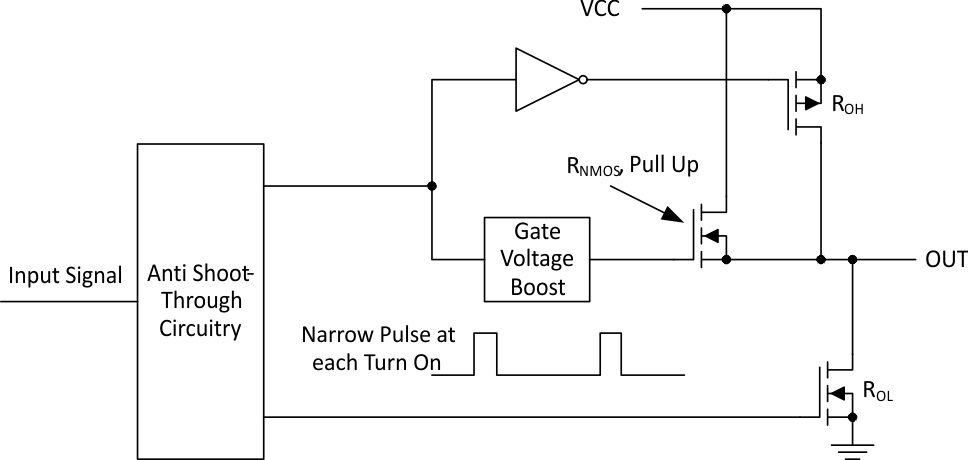
The UCC44273 is capable of delivering 4-A source, 4-A sink (symmetrical drive) at VDD = 12 V. The output stage of the UCC44273 device is illustrated in Figure 7-2. The UCC44273 features a unique architecture on the output stage which delivers the highest peak-source current when most needed during the Miller-plateau region of the power-switch turnon transition (when the power-switch drain/collector voltage experiences dV/dt). The device output stage features a hybrid pullup structure using a parallel arrangement of N-Channel and P-Channel MOSFET devices. By turning on the N-Channel MOSFET during a narrow instant when the output changes state from low to high, the gate-driver device delivers a brief boost in the peak-sourcing current enabling fast turnon.
 Figure 7-2 UCC44273 Gate Driver Output Structure
The ROH parameter (see Section 6.5) is a DC measurement and is representative of the on-resistance of the P-Channel device only, since the N-Channel device is turned on only during output change of state from low to high. Thus the effective resistance of the hybrid pullup stage is much lower than what is represented by ROH parameter. The pulldown structure is composed of a N-Channel MOSFET only. The ROL parameter (see Section 6.5), which is also a DC measurement, is representative of true impedance of the pulldown stage in the device. In the UCC44273, the effective resistance of the hybrid pullup structure is approximately 1.4 × ROL.
The driver-output voltage swings between VDD and GND providing rail-to-rail operation because of the MOS output stage which delivers very low dropout. The presence of the MOSFET-body diodes also offers low impedance to switching overshoots and undershoots. This means that in many cases, external Schottky-diode clamps may be eliminated. The outputs of these drivers are designed to withstand 500-mA reverse current without either damage to the device or logic malfunction.