ZHCSDF1 February 2015 UCD90240
PRODUCTION DATA.
- 1 特性
- 2 应用
- 3 说明
- 4 修订历史记录
- 5 Pin Configuration and Functions
- 6 Specifications
-
7 Detailed Description
- 7.1 Device Overview
- 7.2 Functional Block Diagram
- 7.3
Feature Description
- 7.3.1 TI Fusion GUI
- 7.3.2 PMBUS Interface
- 7.3.3 Rail Setup
- 7.3.4 Rail Monitoring Configuration
- 7.3.5 GPI Configuration
- 7.3.6 Rail Sequence Configuration
- 7.3.7 Fault Responses Configuration
- 7.3.8 GPO Configuration
- 7.3.9 Margining Configuration
- 7.3.10 Pin Selected Rail States Configuration
- 7.3.11 Watchdog Timer
- 7.3.12 System Reset Function
- 7.3.13 Cascading Multiple Devices
- 7.3.14 Voltage Monitoring
- 7.3.15 Status Monitoring
- 7.3.16 Data and Error Logging to EEPROM Memory
- 7.3.17 Black Box First Fault Logging
- 7.3.18 PMBUS Address Selection
- 7.3.19 ADC Reference
- 7.3.20 Device Reset
- 7.3.21 Brownout
- 7.3.22 Device Configuration and Programming
- 7.3.23 Internal Fault Management
- 8 Application and Implementation
- 9 Power Supply Recommendations
- 10Layout
- 11器件和文档支持
- 12机械封装和可订购信息
10 Layout
10.1 Layout Guidelines
- Decoupling capacitors should be placed as close to the device as possible.
- BPCAP decoupling capacitors should be connected as close as possible to pin D6.
- MARGIN pins output fast-edge PWM signals. These signals should be routed away from sensitive analog signals. It is a good practice to place R4 and C1 in Figure 16 as close as possible to the MARGIN pin, minimizing the propagation distance of the fast-edge PWM signals on the PCB. R3 can be placed near the power supply feedback node to isolate the feedback node from noise sources on the PCB. If R4 and C1 cannot be located close to the MARGIN pin, add a 20-Ω to 33-Ω series termination resistor located near the MARGIN pin.
10.2 Layout Example
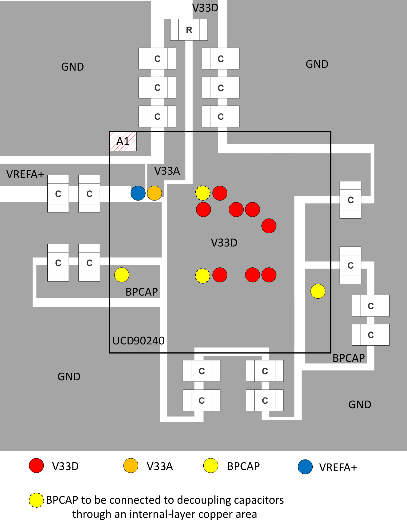
UCD90240 is in a 157-pin BGA package. If UCD90240 is mounted on the top layer, decoupling capacitors can be placed on the bottom layer to make room for top-layer trace routing. The layout example below adopts such a strategy. Figure 35 shows bottom-layer component placement from top-view. In addition to Figure 35, note that:
- A uniform ground plane should be used to connect DVSS, AVSS, and VREFA– pins.
- All four BPCAP pins should be connected to a common internal-layer copper area.
- AVSS and VREFA– pins can be connected to a common internal-layer copper area.
 Figure 35. Bottom-layer Component Placement
 (Top view, UCD90240 is Mounted on Top Layer)