SBOA447 November 2020 ALM2402-Q1 , ALM2402F-Q1 , ALM2403-Q1
4 ALM2403-Q1 Overvoltage Protection Schemes for High Vbat Voltages
Most of the ALM2403-Q1 protection circuits discussed so far involved adding a TVS on the supply pin to prevent over-voltage damage and a Schottky diode with a series output power resistor to guard against the over-current damage – these schemes typically work well but are both bulky and costly solutions. However, there is yet another novel approach that greatly limits the current level under fault conditions (thus eliminates the need for the Schottky diode) without limiting the output voltage swing to rail under normal circuit conditions.
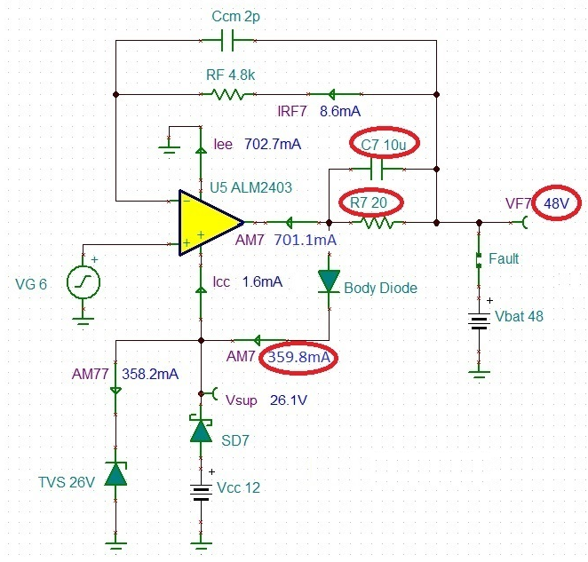
 Figure 4-1 ALM2403-Q1 48 V Battery Fault
Protection
Figure 4-1 ALM2403-Q1 48 V Battery Fault
ProtectionFigure 4-1 shows that under a short to 48 V battery fault condition it may take as much as 20Ω of series output power resistor, R7, to limit the current through the body diode to a safe magnitude. This means that under normal operation, with typical current load of +/-200mA, this would result in additional loss of 8 V of the voltage supply headroom, greatly diminishing power efficiency of the solution. However, if the R7 resistor is placed inside the feedback loop and bypassed with a large, non-polarized capacitor, C7, the resolver normal operation performance is hardly affected.
At the typical frequency of 10kHz used in most automotive resolver excitation applications, the impedance of 10uF bypass capacitor is around 1.6Ω, which lowers the output voltage swing to the rail under +/-200mA peak load by just +/-320mV instead of +/-4 V. This means that there is little need to increase supply voltage, which results in higher efficiency of the resolver solution.
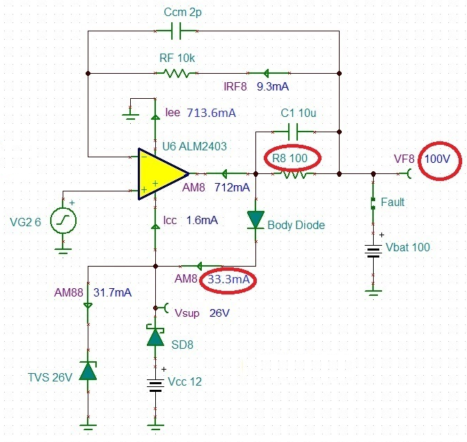
 Figure 4-2 ALM2403-Q1 100V Battery Fault
Protection
Figure 4-2 ALM2403-Q1 100V Battery Fault
ProtectionThe same scheme may easily be employed to protect the ALM2403-Q1 output against a short to a much higher battery voltage, like 100 V, shown in Figure 4-2 above. The only difference between the two fault protections is that it now takes a higher value series power output resistor, R8, to properly limit the current under fault condition. Nevertheless, since the 100Ω series output resistor is similarly bypassed by the same 10uF capacitor, C1, the normal resolver operation of the circuit is hardly effected and thus almost identical as in the case shown in Figure 4-1. It should be noted that the output resistor bypass capacitor’s maximum rated voltage should be sufficient to withstand the DC voltage imposed across it during a fault condition.
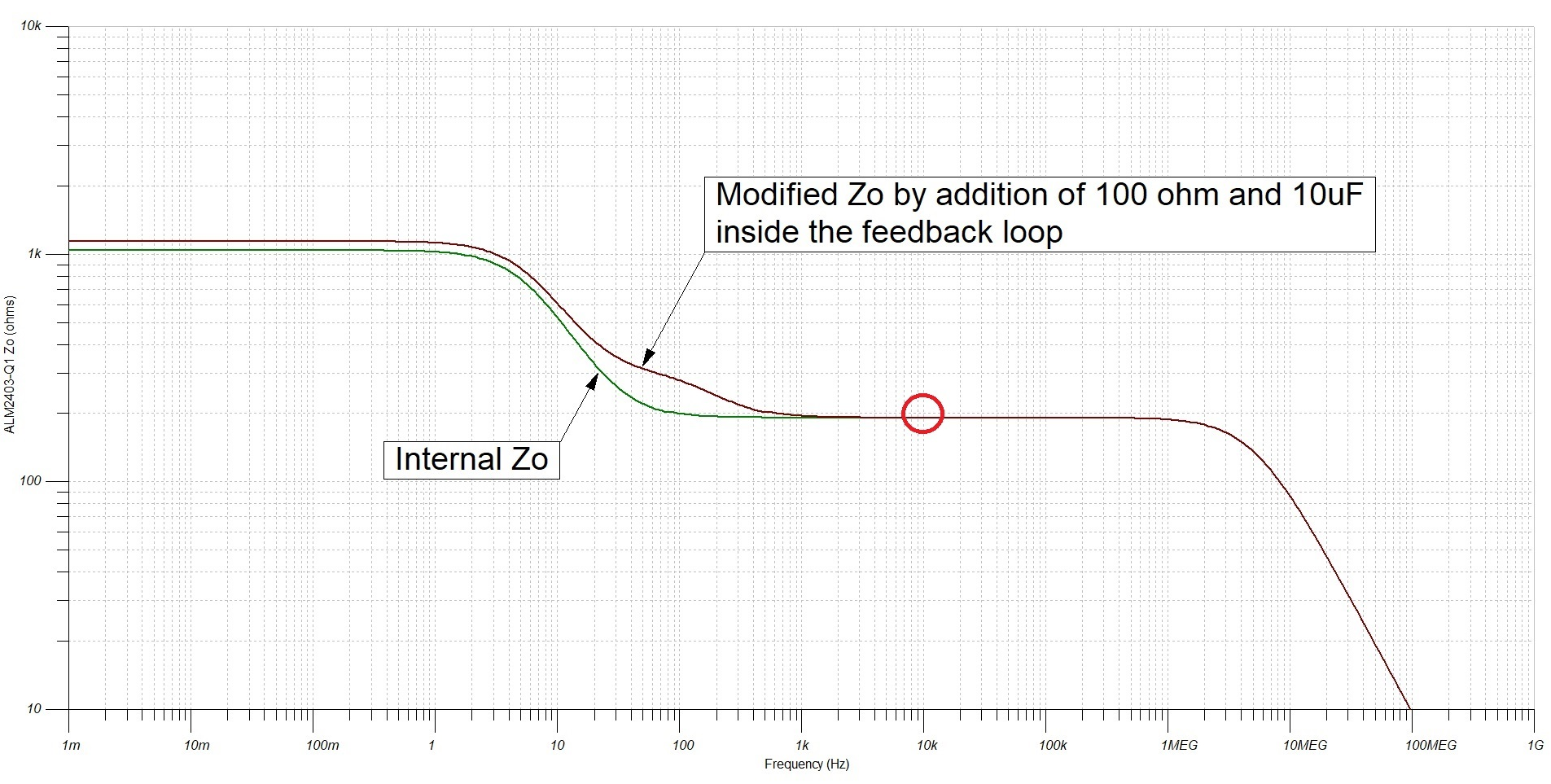
The only other consideration of the effects of adding a large series output resistor paralleled with 10uF capacitor inside the feedback loop has to do with their effect on the modified open-loop output impedance, Zo, which controls the stability of the circuit while driving complex loads. However, as may be seen in the simulation of Zo vs frequency graph shown in Figure 4-3, the R||C inclusion inside the feedback loop hardly makes any difference especially at the 10kHz frequency typically used in most automotive resolver applications. Thus, the circuit is capable of driving the same complex loads as in the case with no additional R||C fault protection circuitry.
 Figure 4-3 ALM2403-Q1 Open-Loop Output
Impedance