SBOS424C March 2008 – November 2015 PGA112 , PGA113 , PGA116 , PGA117
PRODUCTION DATA.
- 1 Features
- 2 Applications
- 3 Description
- 4 Revision History
- 5 Device Comparison
- 6 Pin Configuration and Functions
- 7 Specifications
- 8 Detailed Description
-
9 Applications and Implementation
- 9.1
Application Information
- 9.1.1 Op Amp: Input Stage
- 9.1.2 Op Amp: General Gain Equations
- 9.1.3 Op Amp: Frequency Response Versus Gain
- 9.1.4 Analog MUX
- 9.1.5 System Calibration Using The PGA
- 9.1.6 Driving and Interfacing to ADCs
- 9.1.7 Power Supplies
- 9.1.8 Shutdown and Power-On-Reset (POR)
- 9.1.9 Typical Connections: PGA116, PGA117 (TSSOP-20)
- 9.2 Typical Applications
- 9.1
Application Information
- 10Power Supply Recommendations
- 11Layout
- 12Device and Documentation Support
- 13Mechanical, Packaging, and Orderable Information
8 Detailed Description
8.1 Overview
The PGA112 and PGA113 devices (binary and scope gains) offer two analog inputs, a three-pin SPI interface, and software shutdown in an 10-pin VSSOP package. The PGA116 and PGA117 (binary and scope gains) offer 10 analog inputs, and hardware and software shutdown in a 20-pin TSSOP package.
All versions provide internal calibration channels for system-level calibration. The channels are tied to GND, 0.9 VCAL, 0.1 VCAL, and VREF, respectively. VCAL, an external voltage connected to Channel 0, is used as the system calibration reference. Binary gains are: 1, 2, 4, 8, 16, 32, 64, and 128; scope gains are: 1, 2, 5, 10, 20, 50, 100, and 200.
The PGA uses a SPI interface with daisy-chain capability, a standard serial peripheral interface (SPI). Both SPI Mode 0,0 and Mode 1,1 are supported, as shown in Figure 56 and described in Table 2.
8.2 Functional Block Diagram
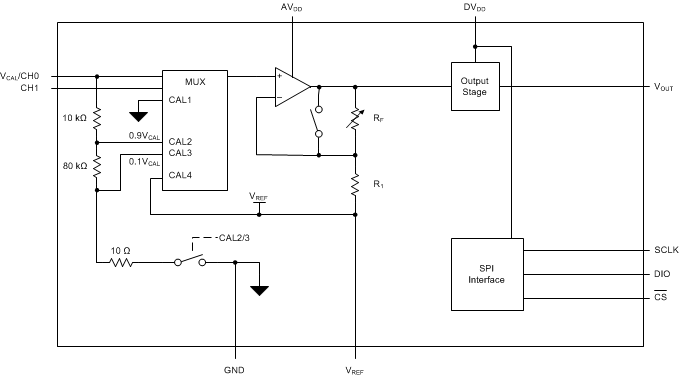
8.3 Feature Description
Featuring low offset, low offset drift and low noise, the PGA11x series provides a flexible analog building block for a variety of applications. The PGA112 and PGA116 offer binary gains of 1, 2, 4, 8, 16, 32, 64, 128 and a 2 channel MUX while the PGA113 and PGA117 offer scope gains of 1, 2, 5, 10, 20, 50, 100, 200 and a 10 channel MUX.
8.4 Device Functional Modes
The PGA112 and PGA113 devices have a software shutdown mode, and the PGA116 and PGA117 devices offer both a hardware and software shutdown mode, see Shutdown and Power-On-Reset (POR) for additional information. The PGA uses a standard serial peripheral interface (SPI). Both SPI Mode 0,0 and Mode 1,1 are supported. More information regarding serial communications, including daisy chaining can be found in Serial Interface Information.
8.5 Programming
Table 1. Frequency Response Versus Gain (CL = 100 pf, RL= 10 kω)
| BINARY GAIN (V/V) | TYPICAL –3-dB FREQUENCY (MHz) |
SLEW RATE-FALL (V/μs) |
SLEW RATE-RISE (V/μs) |
0.1% SETTLING TIME: 4 VPP (μs) |
0.01% SETTLING TIME: 4 VPP (μs) |
SCOPE GAIN (V/V) |
TYPICAL –3-dB FREQUENCY (MHz) |
SLEW RATE-FALL (V/μs) |
SLEW RATE-RISE (V/μs) |
0.1% SETTLING TIME: 4 VPP (μs) |
0.01% SETTLING TIME: 4 VPP (μs) |
|
|---|---|---|---|---|---|---|---|---|---|---|---|---|
| 1 | 10 | 8 | 3 | 2 | 2.55 | 1 | 10 | 8 | 3 | 2 | 2.55 | |
| 2 | 3.8 | 9 | 6.4 | 2 | 2.6 | 2 | 3.8 | 9 | 6.4 | 2 | 2.6 | |
| 4 | 2 | 12.8 | 10.6 | 2 | 2.6 | 5 | 1.8 | 12.8 | 10.6 | 2 | 2.6 | |
| 8 | 1.8 | 12.8 | 10.6 | 2 | 2.6 | 10 | 1.8 | 12.8 | 10.6 | 2.2 | 2.6 | |
| 16 | 1.6 | 12.8 | 12.8 | 2.3 | 2.6 | 20 | 1.3 | 12.8 | 9.1 | 2.3 | 2.8 | |
| 32 | 1.8 | 12.8 | 13.3 | 2.3 | 3 | 50 | 0.9 | 9.1 | 7.1 | 2.4 | 3.8 | |
| 64 | 0.6 | 4 | 3.5 | 3 | 6 | 100 | 0.38 | 4 | 3.5 | 4.4 | 7 | |
| 128 | 0.35 | 2.5 | 2.5 | 4.8 | 8 | 200 | 0.23 | 2.3 | 2 | 6.9 | 10 |
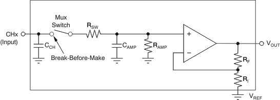 Figure 55. Equivalent Input Circuit
8.6 Serial Interface Information
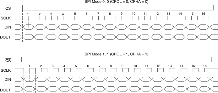 Figure 56. SPI Mode 0,0 And Mode 1,1
Table 2. SPI Mode Setting Description
| MODE | CPOL | CPHA | CPOL DESCRIPTION | CPHA DESCRIPTION |
|---|---|---|---|---|
| 0, 0 | 0 | 0(1) | Clock idles low | Data are read on the rising edge of clock. Data change on the falling edge of clock. |
| 1, 1 | 1 | 1(2) | Clock idles high | Data are read on the rising edge of clock. Data change on the falling edge of clock. |
8.6.1 Serial Digital Interface: SPI Modes
The PGA uses a standard serial peripheral interface (SPI). Both SPI Mode 0,0 and Mode 1,1 are supported, as shown in Figure 56 and described in Table 2.
If there are not even-numbered increments of 16 clocks (that is, 16, 32, 64, and so forth) between CS going low (falling edge) and CS going high (rising edge), the device takes no action. This condition provides reliable serial communication. Furthermore, this condition also provides a way to quickly reset the SPI interface to a known starting condition for data synchronization. Transmitted data are latched internally on the rising edge of CS.
On the PGA116 and PGA117 devices, CS, DIN, and SCLK are Schmitt-triggered CMOS logic inputs. DIN has a weak internal pulldown to support daisy-chain communications on the PGA116 and PGA117 devices. DOUT is a CMOS logic output. When CS is high, the state of DOUT is high-impedance. When CS is low, DOUT is driven as illustrated in Figure 57.
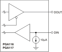 Figure 57. Digital I/O Structure—PGA116 and PGA117
On the PGA112 and PGA113 devices, there are digital output and digital input gates both internally connected to the DIO pin. DIN is an input-only gate and DOUT is a digital output that can give a 3-state output. The DIO pin has a weak 10-μA pulldown current source to prevent the pin from floating in systems with a high-impedance SPI DOUT line. When CS is high, the state of the internal DOUT gate is high-impedance. When CS is low, the state of DIO depends on the previous valid SPI communication; either DIO becomes an output to clock out data or it remains an input to receive data. This structure is shown in Figure 58.
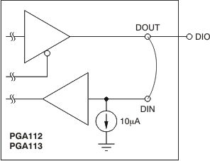 Figure 58. Digital I/O Structure—PGA112 and PGA113
8.6.2 Serial Digital Interface: SPI Daisy-Chain Communications
To reduce the number of I/O port pins used on a microcontroller, the PGA116 and PGA117 support SPI daisy-chain communications with full read and write capability. A two-device daisy-chain configuration is shown in Figure 59, although any number of devices can be daisy-chained. The SPI daisy-chain communication uses a common SCLK and CS line for all devices in the daisy chain, rather than each device requiring a separate CS line. The daisy-chain mode of communication routes data serially through each device in the chain by using its respective DIN and DOUT pins as shown. Special commands are used (see Table 4) to ensure that data are written or read in the proper sequence. There is a special daisy-chain NOP command (No OPeration) which, when presented to the desired device in the daisy-chain, causes no changes in that respective device. Detailed timing diagrams for daisy-chain operation are shown in Figure 63 through Figure 65.
 Figure 59. Daisy-Chain Read and Write Configuration
The PGA112 and PGA113 devices can be used as the last device in a daisy-chain as shown in Figure 60 if write-only communication is acceptable, because the PGA112 and PGA113 devices have no separate DOUT pin to connect back to the microcontroller DIN pin to read back data in this configuration.
 Figure 60. Daisy-Chain Write-Only Configuration
The maximum SCLK frequency that can be used in daisy-chain operation is directly related to SCLK rise and fall times, DIN setup time, and DOUT propagation delay. Any number of two or more devices have the same limitations because it is the timing considerations between adjacent devices that limit the clock speed.
Figure 61 analyzes the maximum SCLK frequency for daisy-chain mode based on the circuit of Figure 59. A clock rise and fall time of 10 ns is assumed to allow for extra bus capacitance that could occur as a result of multiple devices in the daisy-chain.
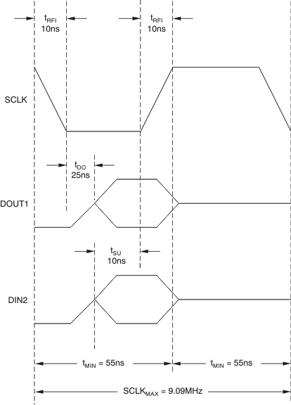 Figure 61. Daisy-Chain Maximum SCLK Frequency
8.6.3 SPI Serial Interface
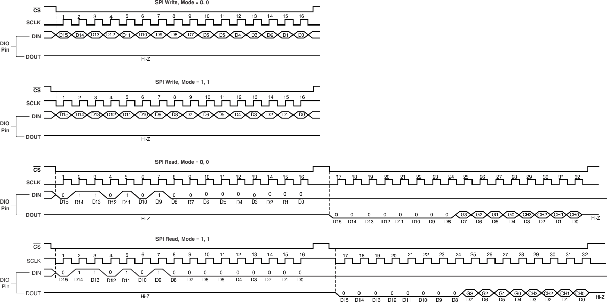 Figure 62. SPI Serial Interface Timing Diagrams
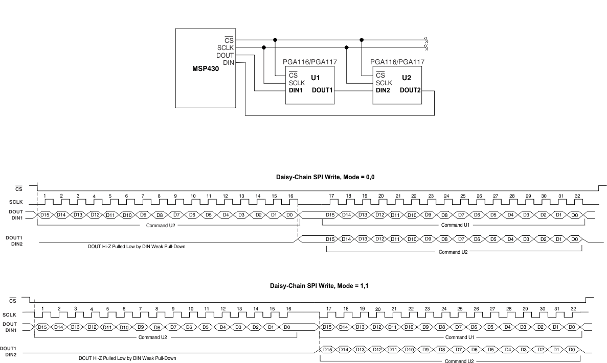 Figure 63. SPI Daisy-Chain Write Timing Diagrams
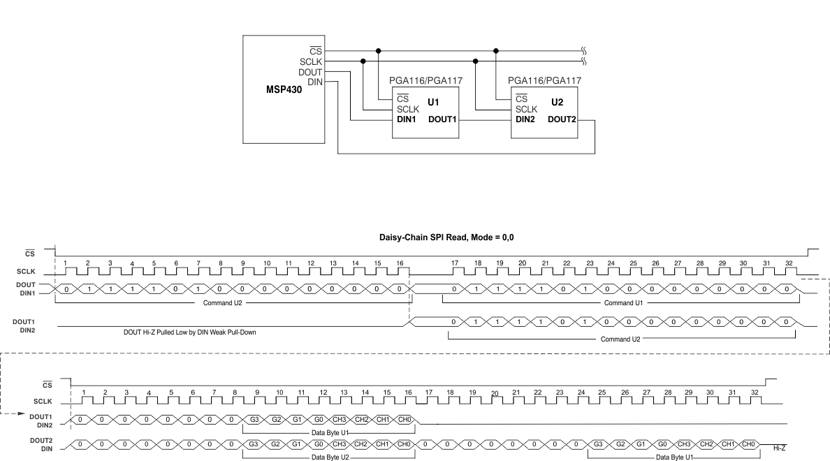 Figure 64. SPI Daisy-Chain Read Timing Diagram (Mode 0,0)
 Figure 65. SPI Daisy-Chain Read Timing Diagram (Mode 1,1)
8.6.4 SPI Commands
Table 3. SPI Commands (PGA112 and PGA113)(1)(2)
| D15 | D14 | D13 | D12 | D11 | D10 | D9 | D8 | D7 | D6 | D5 | D4 | D3 | D2 | D1 | D0 | THREE-WIRE SPI COMMAND | |
|---|---|---|---|---|---|---|---|---|---|---|---|---|---|---|---|---|---|
| 0 | 1 | 1 | 0 | 1 | 0 | 1 | 0 | 0 | 0 | 0 | 0 | 0 | 0 | 0 | 0 | READ | |
| 0 | 0 | 1 | 0 | 1 | 0 | 1 | 0 | G3 | G2 | G1 | G0 | CH3 | CH2 | CH1 | CH0 | WRITE | |
| 0 | 0 | 0 | 0 | 0 | 0 | 0 | 0 | 0 | 0 | 0 | 0 | 0 | 0 | 0 | 0 | NOP WRITE | |
| 1 | 1 | 1 | 0 | 0 | 0 | 0 | 1 | 0 | 0 | 0 | 0 | 0 | 0 | 0 | 0 | SDN_DIS WRITE | |
| 1 | 1 | 1 | 0 | 0 | 0 | 0 | 1 | 1 | 1 | 1 | 1 | 0 | 0 | 0 | 1 | SDN_EN WRITE |
Table 4. SPI Daisy-Chain Commands(1)(2)
| D15 | D14 | D13 | D12 | D11 | D10 | D9 | D8 | D7 | D6 | D5 | D4 | D3 | D2 | D1 | D0 | DAISY-CHAIN COMMAND | |
|---|---|---|---|---|---|---|---|---|---|---|---|---|---|---|---|---|---|
| 0 | 0 | 0 | 1 | 0 | 0 | 0 | 0 | 0 | 0 | 0 | 0 | 0 | 0 | 0 | 0 | NOP | |
| 1 | 1 | 1 | 1 | 0 | 0 | 0 | 1 | 0 | 0 | 0 | 0 | 0 | 0 | 0 | 0 | SDN_DIS | |
| 1 | 1 | 1 | 1 | 0 | 0 | 0 | 1 | 1 | 1 | 1 | 1 | 0 | 0 | 0 | 1 | SDN_EN | |
| 0 | 1 | 1 | 1 | 1 | 0 | 1 | 0 | 0 | 0 | 0 | 0 | 0 | 0 | 0 | 0 | READ | |
| 0 | 0 | 1 | 1 | 1 | 0 | 1 | 0 | G3 | G2 | G1 | G0 | CH3 | CH2 | CH1 | CH0 | WRITE |
Table 5. Gain Selection Bits (PGA112 and PGA113)
| G3 | G2 | G1 | G0 | BINARY GAIN | SCOPE GAIN |
|---|---|---|---|---|---|
| 0 | 0 | 0 | 0 | 1 | 1 |
| 0 | 0 | 0 | 1 | 2 | 2 |
| 0 | 0 | 1 | 0 | 4 | 5 |
| 0 | 0 | 1 | 1 | 8 | 10 |
| 0 | 1 | 0 | 0 | 16 | 20 |
| 0 | 1 | 0 | 1 | 32 | 50 |
| 0 | 1 | 1 | 0 | 64 | 100 |
| 0 | 1 | 1 | 1 | 128 | 200 |
Table 6. MUX Channel Selection Bits
| CH3 | CH2 | CH1 | CH0 | PGA112, PGA113 | PGA116, PGA117 |
|---|---|---|---|---|---|
| 0 | 0 | 0 | 0 | VCAL/CH0 | VCAL/CH0 |
| 0 | 0 | 0 | 1 | CH1 | CH1 |
| 0 | 0 | 1 | 0 | X(1) | CH2 |
| 0 | 0 | 1 | 1 | X | CH3 |
| 0 | 1 | 0 | 0 | X | CH4 |
| 0 | 1 | 0 | 1 | X | CH5 |
| 0 | 1 | 1 | 0 | X | CH6 |
| 0 | 1 | 1 | 1 | X | CH7 |
| 1 | 0 | 0 | 0 | X | CH8 |
| 1 | 0 | 0 | 1 | X | CH9 |
| 1 | 0 | 1 | 0 | X | X(1) |
| 1 | 0 | 1 | 1 | Factory Reserved | Factory Reserved |
| 1 | 1 | 0 | 0 | CAL1(2) | CAL1(2) |
| 1 | 1 | 0 | 1 | CAL2(3) | CAL2(3) |
| 1 | 1 | 1 | 0 | CAL3(4) | CAL3(4) |
| 1 | 1 | 1 | 1 | CAL4(5) | CAL4(5) |