SBOS583B December 2011 – December 2016
PRODUCTION DATA.
7 Detailed Description
7.1 Overview
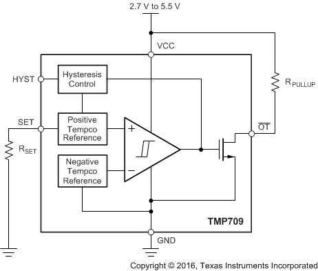
The TMP709 is a fully-integrated, resistor-programmable temperature switch that incorporates two temperature-dependent voltage references and one comparator. One voltage reference exhibits a positive temperature coefficient (tempco), and the other voltage reference exhibits a negative tempco. The temperature at which both voltage references are equal determines the temperature trip point.
The Functional Block Diagram shows the comparator, the NFET open-drain device connected to the OT pin, the positive tempco reference using the external RSET resistor, the negative tempco reference, and the hysteresis control. The voltage of the positive tempco reference is controlled by external resistor RSET.
7.2 Functional Block Diagram

7.3 Feature Description
7.3.1 Temperature Switch
The TMP709 temperature threshold is programmable from 0°C to 125°C and is set by an external 1% resistor from the SET pin to the GND pin. The TMP709 has an open-drain, active-low output structure that easily interfaces with a microprocessor.
The TMP709 reaches the temperature trip point when the voltage from the positive tempco reference exceeds the voltage from the negative tempco reference. This difference causes the output of the comparator to switch from logic 0 to logic 1. The comparator output drives the gate of the NFET open-drain device, and pulls the voltage on the OT pin from logic 1 to logic 0 under these conditions; in other words, the output trips. Furthermore, the logic 1 output from the comparator causes the hysteresis control to increase the voltage of the positive tempco reference by an amount set by the logic setting on the HYST pin (10°C for logic 1 on the HYST pin; 2°C for logic 0 on the HYST pin). Increase the voltage of the positive tempco reference after the TMP709 trips to stop the TMP709 from untripping (voltage on the OT pin changing from logic 0 to logic 1) until the local temperature reduces by the amount set by the HYST pin. After the local temperature reduces, and the voltage from the positive tempco reference is less than the voltage from the negative tempco reference, the output of the comparator switches from logic 1 to logic 0. This condition causes the voltage on the OT pin to change from logic 0 to logic 1 (device untrips).
7.3.2 Hysteresis Input
The HYST pin is a digital input that allows the input hysteresis to be set at either 10°C (when HYST = VCC) or 2°C (when HYST = GND). The hysteresis function keeps the OT pin from oscillating when the temperature is near the threshold. Thus, always connect the HYST pin to either VCC or GND. Other input voltages on this pin can cause abnormal supply currents or a device malfunction.
7.3.3 Set-Point Resistor (RSET)
Set the temperature threshold by connecting RSET from the SET pin to GND. The value of RSET is determined using either Figure 2 or Equation 1:
where
- T = temperature threshold in degrees Celsius.
7.4 Device Functional Modes
The TMP709 device has a single functional mode. Normal operation for the TMP709 device occurs when the power-supply voltage applied across the VCC and GND pins is within the specified operating range of 2.7 V to 5.5 V.