SLAA719 August 2016 TPA3221 , TPA3244 , TPA3245 , TPA3250 , TPA3251 , TPA3255 , TPA3255-Q1
2 Input Stage with Ground Plane
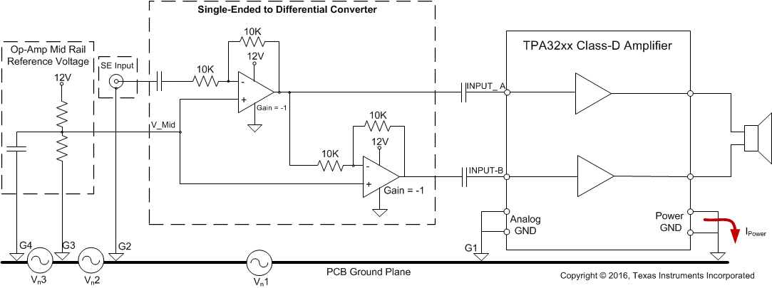
Now suppose that all of the ground points for the input stage are tied to the ground plane at the most convenient locations, as typically done in PCB layout (Figure 2).
At high output power, the ground plane used for the TPA32xx amplifier will start to see heavy current flow and switching noise. This is generally worse at lower audio frequencies where the sustained amplitude of the audio signal peaks is longer when compared to higher frequency signals. This can cause lots of noise on the ground plane.
 Figure 2. SE to Diff Input Stage Ground Plane Noise
 Due to the heavy current flow into the ground plane as represented by the arrow “Ipower” noise voltages Vn1, Vn2, and Vn3 develop across the ground plane. Therefore, the ground nodes for the input stage G2, G3, and G4 will all be at different potentials relative to the TPA32xx amplifier analog ground reference G1.
Since our Op-amp input stage is not truly differential with poor CM rejection, signal imbalance is inevitable. It is likely that a differential noise voltage due to Vn1, Vn2, and Vn3 develop between “Input_A” and “Input_B” and is amplified by the TPA32xx amplifier.
This results in degraded low frequency audio performance.