SLUA778A June 2016 – July 2016 UCC21520 , UCC21520-Q1 , UCC21540
4.2 Schematic and PCB Layout Recommendations when Paralleling Output Channels
To maintain the optimal performance of the UCC21520 with output channel in parallel, it is recommended to follow the following schematic and PCB layout design considerations,
- Short the INA and INB as close to the device as possible to make sure there is little delay introduced between the two signal inputs.
- Use the same bypassing capacitor for channel A and channel B respectively to minimize the timing imbalance introduced due to parasitic inductance.
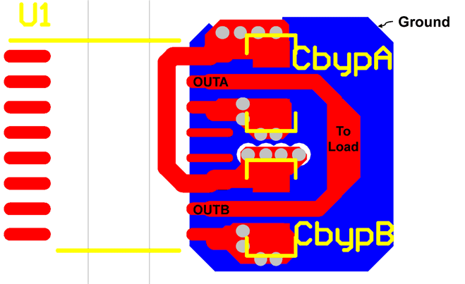
- Make sure the PCB layout are symmetrical between channel A output and channel B output, refer to Figure 16. More PCB layout information can be found in UCC21520 datasheet.
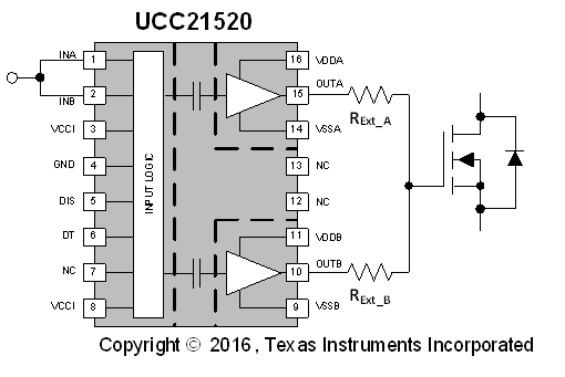
- If the external output resistor is used for system trade-offs, it is recommended to have two resistors with the same resistance value placed in output A and output B to further minimize the parasitic inductance introduced channel imbalance, refer to Figure 17.
 Figure 16. Layout Example for Paralleling UCC21520 Two Output Channels
  Figure 17. Paralleling UCC21520 Two Output Channels with External Resistor