SLUAAC2 March 2021 TPS628510 , TPS628511 , TPS628512
4 Pin Failure Mode Analysis (Pin FMA)
This section provides a Failure Mode Analysis (FMA) for the pins of the TPS62851x. The failure modes covered in this document include the typical pin-by-pin failure scenarios:
- Pin short-circuited to Ground (see Table 4-2)
- Pin open-circuited (see Table 4-3)
- Pin short-circuited to an adjacent pin (see Table 4-4)
- Pin short-circuited to VIN (see Table 4-5)
Table 4-2 through Table 4-5 also indicate how these pin conditions can affect the device as per the failure effects classification in Table 4-1.
| Class | Failure Effects |
|---|---|
| A | Potential device damage that affects functionality |
| B | No device damage, but loss of functionality |
| C | No device damage, but performance degradation |
| D | No device damage, no impact to functionality or performance |
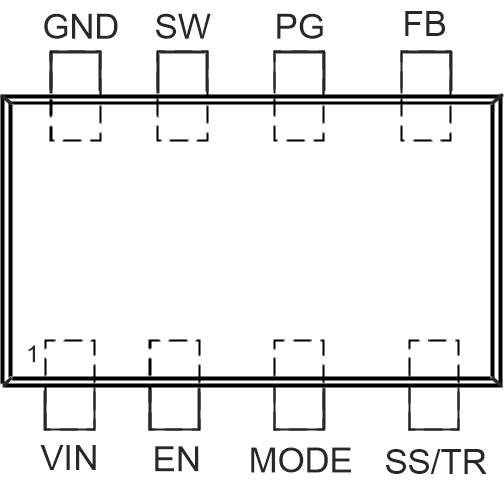
Figure 4-1 shows the TPS62851x pin diagram. For a detailed description of the device pins please refer to the 'Pin Configuration and Functions' section in the TPS62851x datasheet.
 Figure 4-1 Pin Diagram
Following are the assumptions of use and the device configuration assumed for the pin FMA in this section:
- The device is operating in the typical application, please refer to the 'Simplified Schematics' on the 1st page in the TPS62850x datasheet.
| Pin Name | Pin No. | Description of Potential Failure Effect(s) | Failure Effect Class |
|---|---|---|---|
VIN | 1 | Device does not power up | B |
EN | 2 | Intended functionality | D |
MODE/SYNC | 3 | Intended functionality | D |
SS/TR | 4 | Device not functional | D |
FB | 5 | Open loop operation and device performance degradation | C |
PG | 6 | Intended functionality | D |
SW | 7 | Potential device damage | A |
GND | 8 | No effect | D |
| Pin Name | Pin No. | Description of Potential Failure Effect(s) | Failure Effect Class |
|---|---|---|---|
VIN | 1 | Device does not power up | B |
EN | 2 | Undetermined device operation; Device might power up or not | B |
MODE/SYNC | 3 | Undetermined device operation | B |
SS/TR | 4 | Intended functionality | D |
FB | 5 | Device not functional; Open loop operation | B |
PG | 6 | Intended functionality | D |
SW | 7 | Device not functional; Open loop operation | B |
GND | 8 | Potential device damage | A |
| Pin Name | Pin No. | Shorted to | Description of Potential Failure Effect(s) | Failure Effect Class |
|---|---|---|---|---|
VIN | 1 | EN | Intended functionality | D |
EN | 2 | MODE/SYNC | Intended functionality | D |
MODE/SYNC | 3 | SS/TR | Undetermined device operation | C |
FB | 5 | PG | Device not functional; Open loop operation | B |
PG | 6 | SW | Potential internal device damage | A |
SW | 7 | GND | Potential internal device damage | A |
| Pin Name | Pin No. | Description of Potential Failure Effect(s) | Failure Effect Class |
|---|---|---|---|
VIN | 1 | Intended functionality | D |
EN | 2 | Intended functionality; Device enabled | D |
MODE/SYNC | 3 | Intended functionality; FPWM mode | D |
SS/TR | 4 | Intended functionality | D |
FB | 5 | Device not functional; Open loop operation | B |
PG | 6 | Potential device damage | A |
SW | 7 | Potential device damge | A |
GND | 8 | Device not functional | B |