SLUAAF1 May 2021 TPS62933
4 SOT 583 Package Layout Guideline
TPS62933 uses FCOL SOT583 package whose size is 1.6mm×2.1mm. It is rather small and doesn’t have a thermal pad. In order to improve the thermal performance, on time resistor of the FET is designed to have a small value, so that the power loss of the chip can be reduced. Also, PCB design should be optimized to achieve good thermal dissipation.
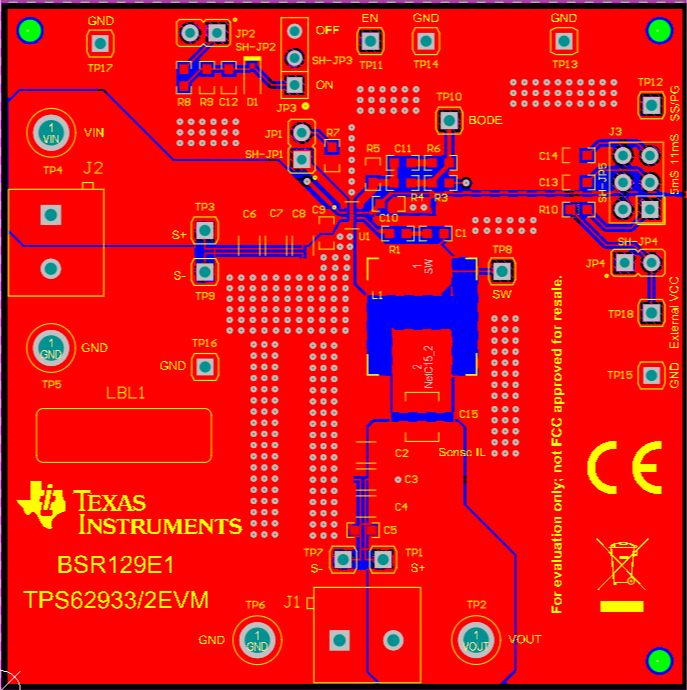
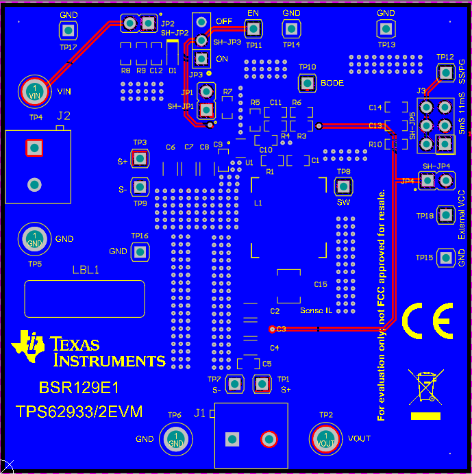
A 4-layer PCB is helpful for thermal dispassion, TI’s SOT583 solution can support a 2-layer application, TI's EVMs use a 2-layer PCB. The typical application circuit of the TPS62933 device is shown in Figure 4-1 and a layout image is provided in Figure 4-2 and Figure 4-3.
 Figure 4-1 Typical Application Circuit of
TPS62933 Device
 Figure 4-2 Top Layer of TPS62933 EVM
 Figure 4-3 Bottom Layer of TPS62933 EVM
The layout in Figure 4-2 and Figure 4-3 is for reference. In some PCB designs, the top and bottom layer may not have so much space. In those cases, IC pins can be connected with vias to copper planes in the inner layers. It is important to realize that in FCOL packages, all IC pins are potential heat conductors and good a thermal connection to PCB copper planes can enhance the thermal cooling effect.
The following list, provides the layout priority:
- VIN and GND traces should be as wide as possible to reduce trace impedance. The wide areas provide better heat dissipation.
- The input capacitor and output capacitor should be placed as close to the device as possible to minimize trace impedance.
- Provide sufficient vias for the input capacitor and output capacitor.
- Keep the SW trace as physically short and wide as practical to minimize radiated emissions.
- Do not allow switching current to flow under the device.
- A separate VOUT path should be connected to the upper feedback resistor.
- Make a Kelvin connection to the GND pin for the feedback path.
- The voltage feedback loop should be placed away from the high-voltage switching trace, and would preferably have a ground shield.
- The trace of the VFB node should be as small as possible to avoid noise coupling.
- The GND trace between the output capacitor and the GND pin should be as wide as possible to minimize its trace impedance.
For a 4-layer PCB, put your signal wire at layer 2 or layer 3, make sure the bottom layer GND does not separate by the line, this will increase thermal dissipation. Also, add more GND via to make all GND in each layer connect together. TI suggests pouring GND polygon for the top layer and the bottom layer.