SLUAAH1 December 2021 UCC24624
2.1 Typical Configuration
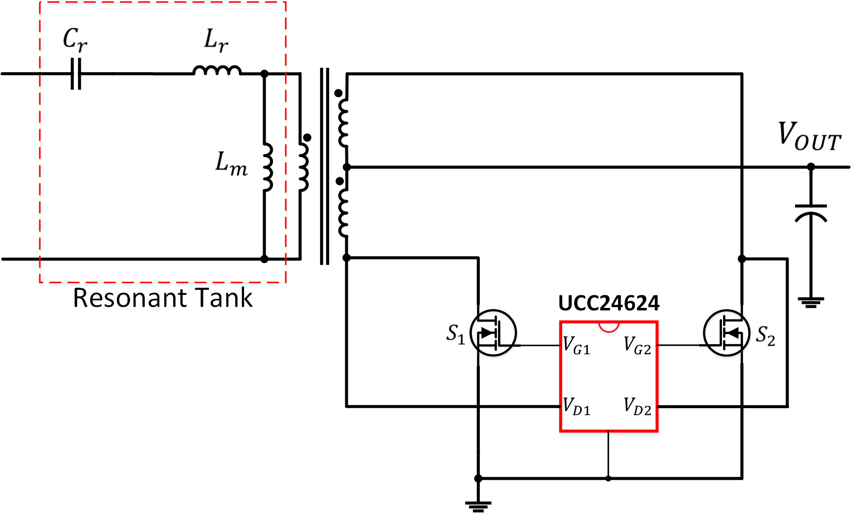
A typical configuration of UCC24624 is shown in Figure 2-1. The UCC24624 provides two high current gate drive outputs, each capable of driving one or N channel power MOSFETs. Each gate driver is controlled separately and an interlock logic circuit prevents the two synchronous rectifiers from being on at the same time.
The control scheme in UCC24624 switches on each SR MOSFET when its VDS falls below -265mV turn-on threshold, and turns it off when VDS rises above the turn-off threshold. The turn-off threshold could be adjusted to maximizing the conduction time of the SR MOSFETs to compensate the offset voltage caused by the parasitic inductance.
 Figure 2-1 UCC24624 Typical Application Schematic