SLUAAL3 July 2022 UCC28C50-Q1 , UCC28C51-Q1 , UCC28C52-Q1 , UCC28C53-Q1 , UCC28C54-Q1 , UCC28C55-Q1 , UCC28C56H-Q1 , UCC28C56L-Q1 , UCC28C57H-Q1 , UCC28C57L-Q1 , UCC28C59-Q1
3 Start-Up Circuitry and Comparisons
To satisfy functional safety during the regenerative braking test and to limit the bus voltage from charging above an unsafe level when the vehicle is towed or pushed, the auxiliary supply must have a total startup time on the order of hundreds of milliseconds. If the controller uses a simple high voltage resistor string to bias VDD during startup, low resistance is needed to charge the VDD capacitor above the controller UVLO threshold. The resistor string will continue to consume power during normal operation, which reduces efficiency and increases standby power. Standby power is a critical requirement in battery-operated systems since it affects the range of an electric vehicle. Therefore, an external, active start-up circuit is recommended.
Figure 3-1 shows a well-known active start-up circuit using a high-voltage BJT (or enhancement-mode MOSFET) with 1.2-kV voltage rating or above. Figure 3-2 shows a novel, alternative startup circuit with two 600-V depletion mode MOSFETs in series. The following discussion will briefly discuss the design and operation of each circuit and then provide comparisons.
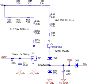 Figure 3-1 Typical 1.2-kV NPN-based Active Start-up
Circuit
Figure 3-1 Typical 1.2-kV NPN-based Active Start-up
CircuitTo power up at low VIN (40 V) within the maximum startup time (tSS, MAX), the NPN-based active startup circuit must provide high enough startup current to charge the VDD capacitor (C12) above VDDON and also deliver the startup current of the PWM controller, ISTART-UP(Controller). This startup requirement sets the maximum value of the total current limiting resistance (RC,MAX) connected from VIN to the collector of the NPN. The trade-off is the resistor size and cost to handle the pulsed current, especially at high VIN (1000V).
During component selection, surge rated resistors with relatively high power handling capability are needed, such as the CRGP Series from TE Connectivity. The 2010 size resistor (typically 1.25 W) from this series is rated for 20-30 W for 100 ms. The collector resistors must be chosen to withstand the power dissipated at the highest VIN (1000 V). Also, multiple resistors in series are required to distribute the maximum input voltage without exceeding the individual voltage rating of each resistor (200 V per resistor).
Lastly, the NPN transistor must receive adequate base current and have a high enough current gain to deliver the previously mentioned current to the VDD capacitor at low VIN. The base current, derived from a second resistor string, increases the standby power and the total power loss of the circuit shown in Figure 3-1 at 1 kV is (1 kV)2 / (6x 750 kΩ) = 220 mW. To guarantee high current gain for lowering power consumption from base current at high VIN and for providing sufficient collector current at low VIN a Darlington transistor was selected, rated for 1.2 kV. Due to the special component selection, the smallest package size option is TO-220, which is over-sized for high voltage startup function. Besides, the component cost and footprint are compromised as well.
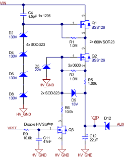 Figure 3-2 Miniature Active Startup
Circuit Using Stacked 600-V Depletion Mode MOSFETs
Figure 3-2 Miniature Active Startup
Circuit Using Stacked 600-V Depletion Mode MOSFETsThe circuit in Figure 3-2 utilizes two 600V depletion mode MOSFETs (2x BSS126). The depletion mode MOSFET conducts when no gate voltage is applied and begins to turn off as the VGS voltage becomes more and more negative. It is completely off when VGS is below the turn-off threshold. The characteristics of the depletion mode FET make it well suited to implementing a current source for high-voltage startup. It is difficult to find a low-cost and small-size depletion MOSFET with 1.2-kV rating, but there are wide variety of selection in 600V to 800V domain. Therefore, the new stacked depletion MOSFET configuration with the proposed gate clamp circuit will evenly distribute the voltage stress from the 1 kV input voltage.
First, let’s look at the operation of Q1. Notice the four 130-V Zener diodes; D2, D4, D6 and D8. Their combined Zener voltage is 520 V. Next, think of R1 as a pull-up resistor to VIN that provides current to the Zener diodes. With that in mind, it’s obvious that these diodes will be off if VIN < 520V. Now, as VIN rises above 520 V, the voltage at the source of Q1 will be clamped slightly above 520 V, let’s say 521 V. In effect Q1 is biased such that the maximum voltage presented to Q2 is 521 V. The VDS voltage of Q1 is VIN – 520 V. At 1000 VIN the VDS of Q2 will be 521 V and VDS of Q1 will be 479 V.
Next, let’s look at the operation of Q2. For now, let’s say D5 is a 22-V redundant (safety) clamp to limit the maximum value of VDD in case Q3 were in a single fault situation and could not shut down Q2. So, for normal operation it’s practical to assume D5 is off. When VDD < VDD,ON, Q3 is also off because the controller has not been powered up and VREF = 0V. R3 is a pull-up resistor (similar to R1 for Q1) that biases D9 on in the forward direction during HV startup. As shown in Figure 3-3, the majority of current flows from the source of Q2 through R5 and charges the 22 µF capacitor on VDD. We can draw the following diagram and use KVL around the loop formed by R3, D9, and R5. Then, the soft start time requirement sets the maximum value of R5, the current limiting resistor.
 Figure 3-3 Solving for the Output
Current, Io
Figure 3-3 Solving for the Output
Current, IoTypical values for VF(D9) and VTH(Q2) are 0.3 V and 1.0 V, respectively. With this information we can solve for Io: (0.3 V + 1.0 V) / 1 kΩ = 1.3 mA. Notice this current does not depend on VIN so it will be constant over the entire range of VIN. The power dissipated by the current limit resistor, (1.3 mA)2 x 1 kΩ = 1.7 mW, is very low for the entire VIN range so the resistor can be quite small, 0603 size.
In both the NPN and Depletion Mode circuits, Q3 functions as a simple switch controlled by VREF from the controller to shut down the HV startup circuit. When Q3 turns on Zener diode D9 is reverse biased and clamps the VGS voltage of Q2 to about ‒18 V. In all cases, shutting down the HV startup circuit reduces power and improves efficiency. Biasing the zener string only requires few µA. The power consumption of Figure 3-2 can be derived as [VTH(Q1) / R1 + VTH(Q2) / R3] x VIN. For 1-V VTH and a 1 MΩ resistors, the power loss at 1 kV is only 1 mW. Compared to the 220 mW consumption of the NPN startup circuit, the standby power is greatly reduced.
C4 is a feedforward capacitor from VIN to the (520-V) zener string. This capacitor speeds up the zener string response in the event VIN changes very quickly (dVIN/dt < 10 V/ns) to maintain even distribution of the voltage stress between the two depletion mode MOSFETs. This capacitor typically should be 1-2 pF, but should be rated for at least 630 V.
Figure 3-4 is a simulation of the depletion mode startup circuitry with VIN ramping up to 800 V in 100 ms. Notice the VDS of Q1 is limited to 280 V and VDS of Q2 is limited to 520 V (the total Zener voltage). Also, the output current is 1.34 mA, as predicted. The VDD voltage rises linearly for 300 ms to 18.27 V.
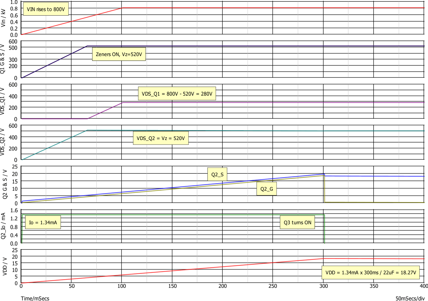 Figure 3-4 Simulation of the Depletion
Mode Startup Circuit, VIN = 800 V
 Figure 3-5 is a simulation when Q3 does not turn on due to single fault event. VDD and VSG_Q2 rise until the 22-V Zener (D5) turns on. At this instant VDD is limited to 22.7 V, a benign value. Without D5 the VDD voltage would rise to a destructive voltage.
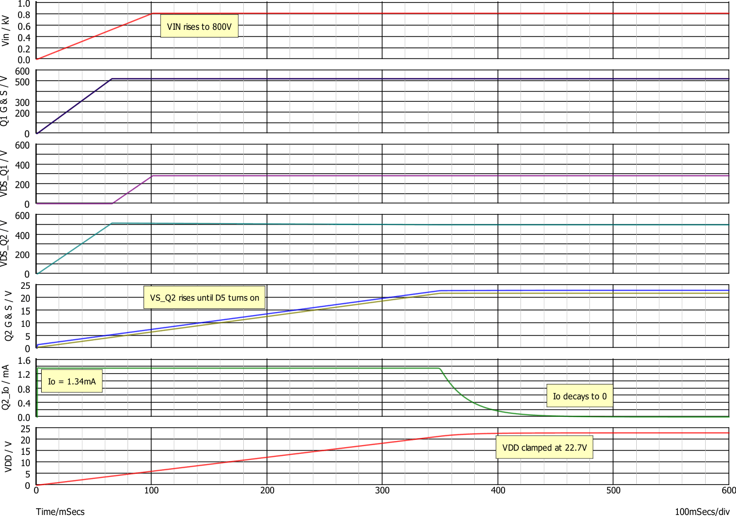 Figure 3-5 Simulation of the Depletion
Mode Startup Circuit, VIN = 800 V
Figure 3-5 Simulation of the Depletion
Mode Startup Circuit, VIN = 800 VThe waveforms in Figure 3-6 to Figure 3-9 are plots measured for both the NPN and Depletion Mode active startup circuits at 50 VIN, 1.3-A load and 800 VIN, 2.7-A load. The total startup time of the NPN based circuit varies from 254 ms at 50 VIN to only 44ms at 800 VIN, a change of 210 ms. The startup time of the Depletion Mode circuit varies from 254 ms to 243 ms, a change of only 11 ms (4.3%)! The performance of the Depletion Mode circuit correlates very well to the simulations.
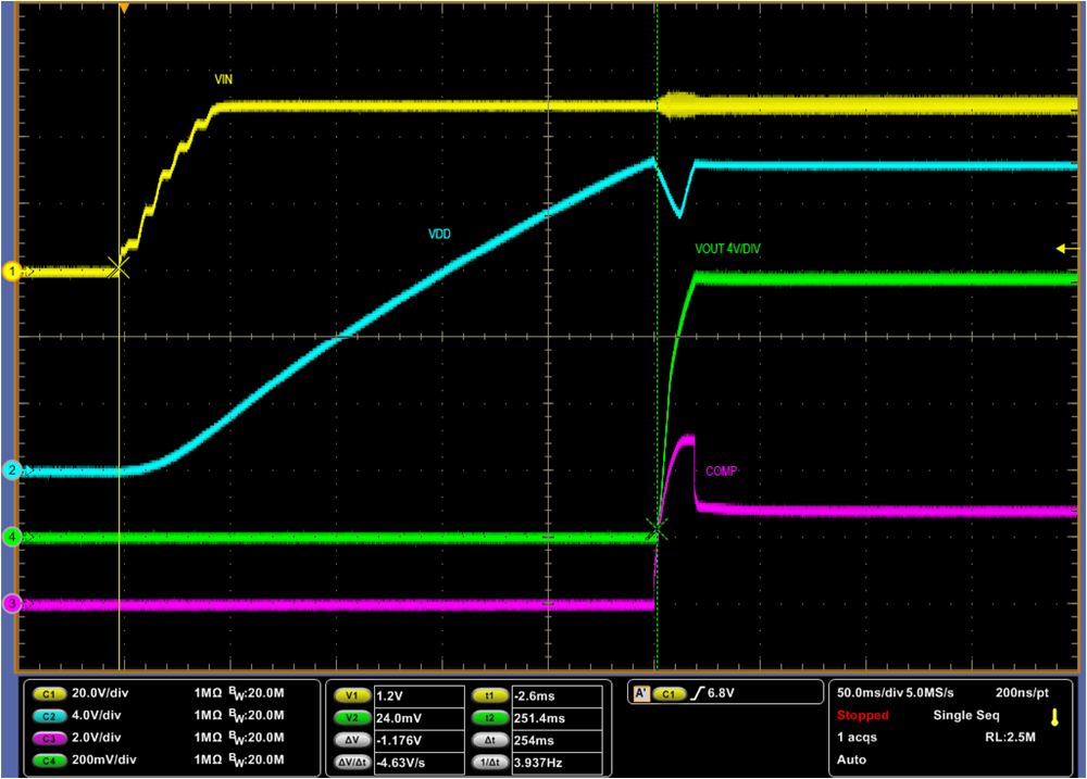
| Total soft start time is 254 ms. |
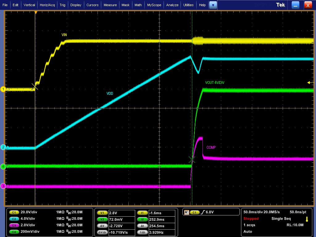
| Total soft start time is 254 ms. |
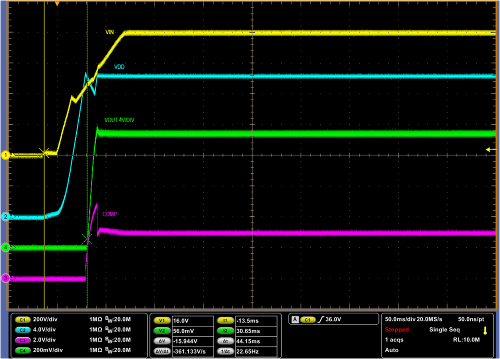
| Total soft start time is 44ms, ∆= -210 ms. |
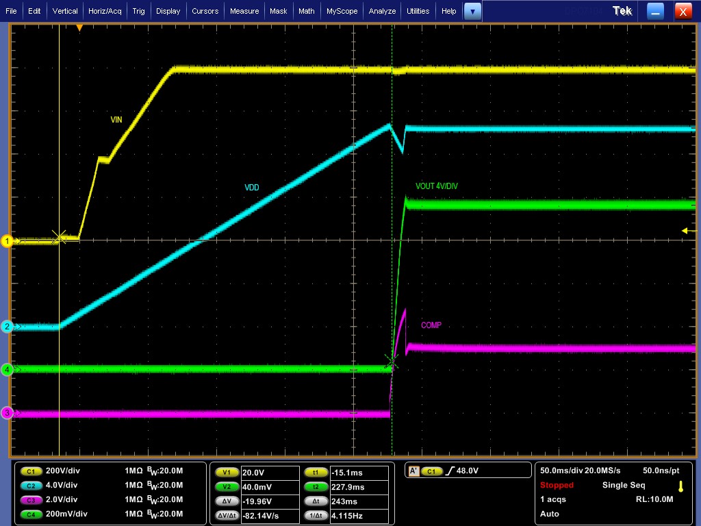
| Total soft start time is 243 ms, ∆= -11 ms. |
Figure 3-10 and Figure 3-11 are physical comparisons of components required for the NPN and Depletion Mode HV startup circuits. The NPN active startup components require 0.64 in2. The depletion mode active startup components require only 0.19 in2. The NPN based circuitry requires at least 3.4x the PCB area, probably more after placing and routing the higher current traces associated with the NPN circuit. Note: the shutdown FET (Q3) and its associated components are common to both solutions so it was omitted from the comparisons.
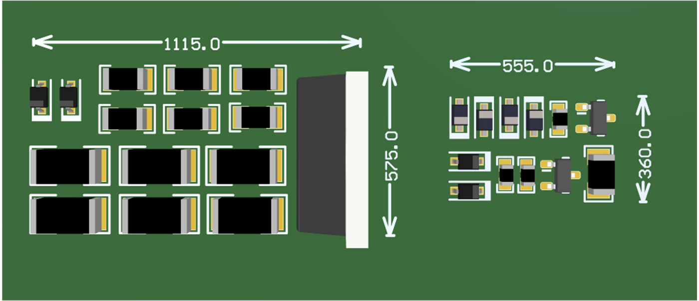 Figure 3-10 2D View Comparing the
Area of the Startup Circuits
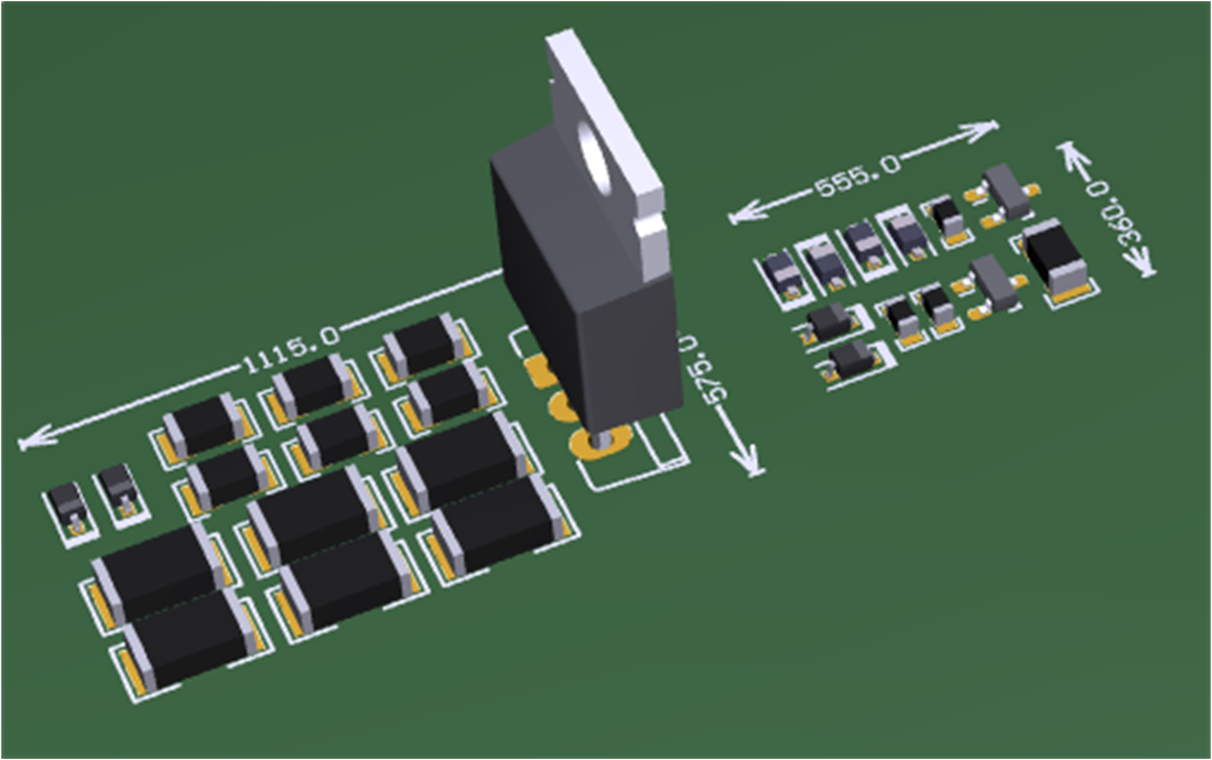 Figure 3-11 3D View Comparing the
Heights of the Startup Circuits
Figure 3-11 3D View Comparing the
Heights of the Startup CircuitsTable 3-1 is a cost comparison between the NPN and Depletion Mode HV startup circuits.
| COMPONENT | UNIT COST | NPN-BASED CIRCUIT | DEPLETION MODE CIRCUIT |
|---|---|---|---|
| 1.2-kV NPN in TO-220 | $1.10 | 1 | |
| 600-V depletion mode MOSFETs in SOT-23 | $0.12 | 2 | |
| 2010-size surge-rated resistors | $0.05 | 6 | |
| 1206-size resistors | $0.015 | 6 | |
| 0603-size resistors | $0.005 | 3 | |
| Zener/Schottky diode in SOD-223 | $0.04 | 2 | 6 |
| 1206-size 630-V capacitor | $0.04 | 1 | |
| Total Cost: | $1.57 | $0.54 | |