SLVA704 June 2015 INA209 , INA219 , INA220 , INA220-Q1 , INA223 , INA226 , INA226-Q1 , INA228 , INA228-Q1 , INA230 , INA231 , INA233 , INA234 , INA237 , INA237-Q1 , INA238 , INA238-Q1 , INA3221 , INA3221-Q1 , LM8323 , LM8325-1 , LM8327 , LM8328 , LM8330 , LM8333 , LM8335 , OPT3001 , OPT3004 , P82B715 , P82B96 , PCA6107 , PCA9306 , PCA9306-Q1 , PCA9515A , PCA9515B , PCA9518 , PCA9534 , PCA9534A , PCA9535 , PCA9536 , PCA9538 , PCA9539 , PCA9543A , PCA9544A , PCA9545A , PCA9546A , PCA9548A , PCA9554 , PCA9554A , PCA9555 , PCA9557 , PCF8574 , PCF8574A , PCF8575 , PCF8575C , TCA4311A , TCA5405 , TCA6408A , TCA6416A , TCA6418E , TCA6424A , TCA6507 , TCA8418 , TCA8418E , TCA8424 , TCA9406 , TCA9509 , TCA9517 , TCA9517A , TCA9534 , TCA9534A , TCA9535 , TCA9538 , TCA9539 , TCA9539-Q1 , TCA9543A , TCA9544A , TCA9545A , TCA9546A , TCA9548A , TCA9554 , TCA9554A , TCA9555 , TCA9617A , TCA9617B , TCA9800 , TCA9801 , TCA9802 , TCA9803
2.3 Acknowledge (ACK) and Not Acknowledge (NACK)
Each byte of data (including the address byte) is followed by one ACK bit from the receiver. The ACK bit allows the receiver to communicate to the transmitter that the byte was successfully received and another byte may be sent.
Before the receiver can send an ACK, the transmitter must release the SDA line. To send an ACK bit, the receiver shall pull down the SDA line during the low phase of the ACK/NACK-related clock period (period 9), so that the SDA line is stable low during the high phase of the ACK/NACK-related clock period. Setup and hold times must be taken into account.
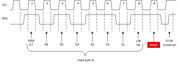
When the SDA line remains high during the ACK/NACK-related clock period, this is interpreted as a NACK. There are several conditions that lead to the generation of a NACK:
- The receiver is unable to receive or transmit because it is performing some real-time function and is not ready to start communication with the master.
- During the transfer, the receiver gets data or commands that it does not understand.
- During the transfer, the receiver cannot receive any more data bytes.
- A master-receiver is done reading data and indicates this to the slave through a NACK.
 Figure 7. Example NACK Waveform