SLVAFE5 September 2022 TPS92610-Q1 , TPS92611-Q1 , TPS92612-Q1 , TPS92613-Q1
3.3 Test Setup
The proposed fault detection circuit was tested utilizing the TPS92611-Q1 and ATL431LI-Q1 EVMs. Figure 3-6 illustrates the block diagram of how the boards were connected for testing.
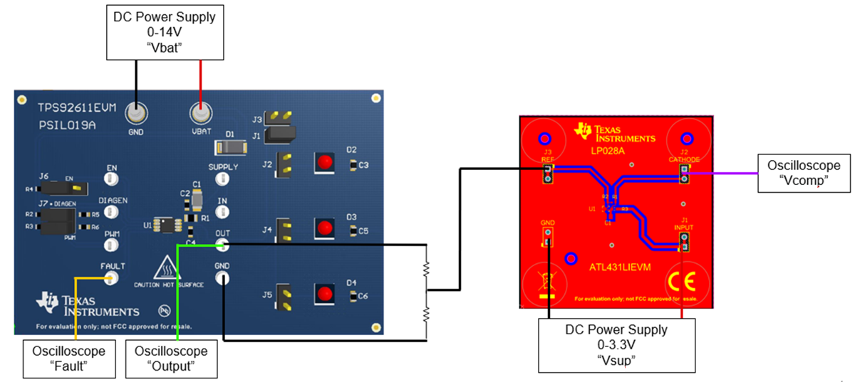 Figure 3-6 Test Setup Block Diagram
The two EVMs were connected through an external resistor ladder and the proper supplies were utilized are shown. Additionally, the test points taken are labeled as shown in the Figure 3-7. The EVMs had multiple jumpers that allowed the testing of each fault condition. For more information on the TPS92611-Q1 EVM, see the TPS92611-Q1 Evaluation Module and ATL431 Adjustable Shunt Regulator EVM user guides.
Figure 3-7 illustrates how the test setup was utilized during testing.
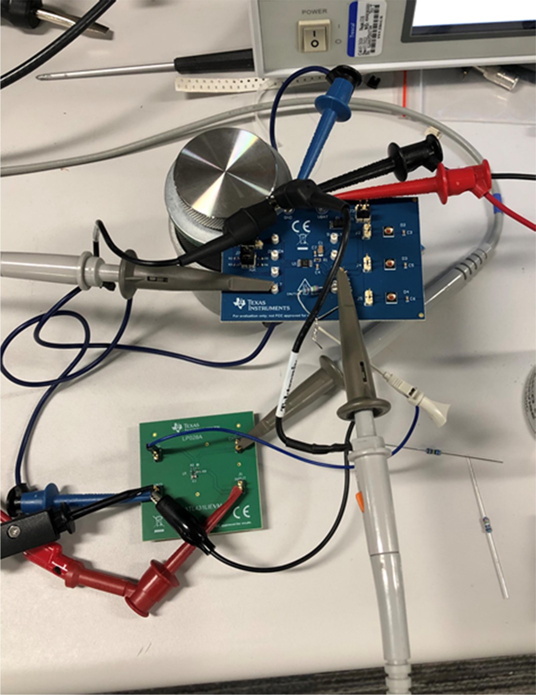 Figure 3-7 Lab Test Setup
In the test setup, the Q1 BJT was not included on the cathode of the ATL431LI-Q1 device so the Vcomp results are going to be inverted of what Figure 2-7 and Table 3-1 show. In addition, the output for low is about 2.5 V instead of ground and the output for high is still a standard 3.3 V. Table 3-2 is included with an inverted Vcomp to assist the comparison of the truth table and scope shots provided.
| Condition | PWM | nFault | Comparator Output (Vcomp) |
|---|---|---|---|
Normal Operation | L | H | L |
H | H | L | |
Short to GND, Overtemperature | L | L | L |
H | L | H | |
Short to Vbat | L | L | L |
H | L | H | |
Open Load | L | H | H |
H | L | H |
Testing was conducted under multiple circumstances to verify that the fault detection circuit behaved as expected. Figure 3-8 illustrates the device under normal operation with the PWM pin on.
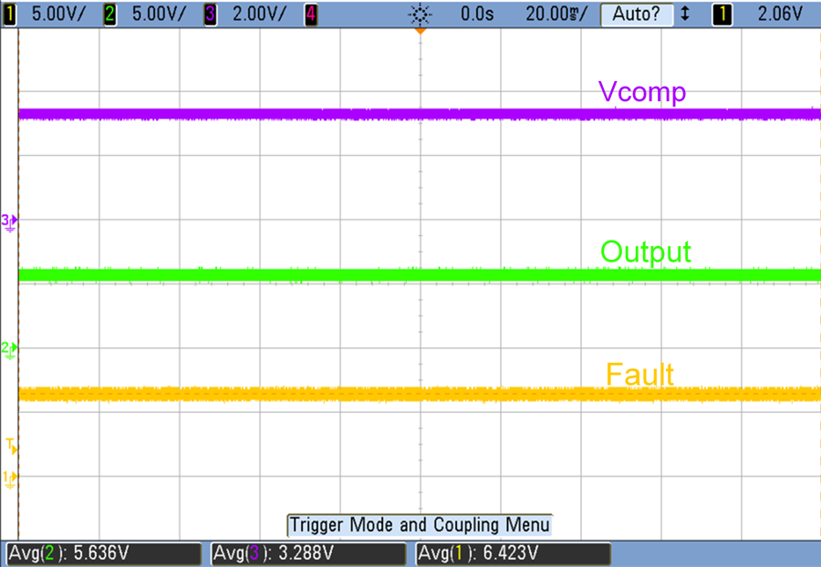 Figure 3-8 Normal Operation
Under normal operation the fault pin stays high. With three LEDs connected to the TPS92611-Q1 there is a constant output of approximately 5.4 V. Additionally, due to no BJT in the testing circuit the Vcomp stays high. Figure 3-9 illustrates device behavior when a SG fault occurs.
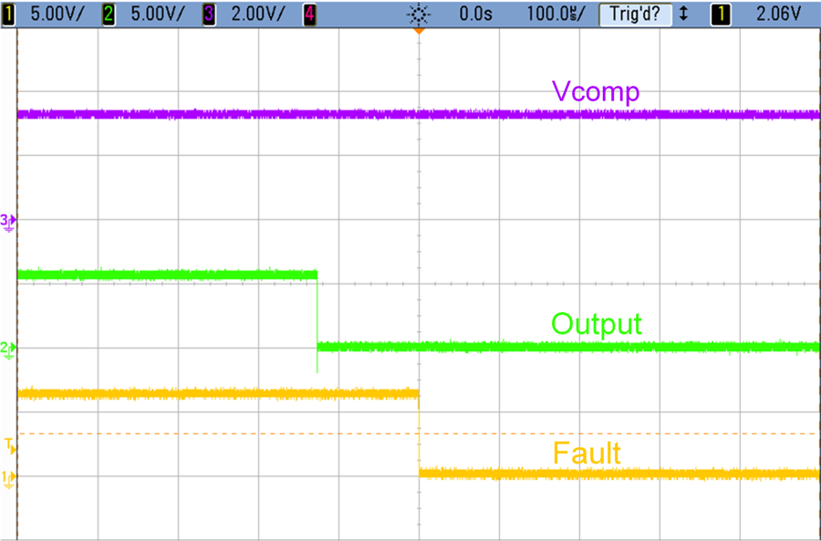 Figure 3-9 Short-to-Ground Fault
When the SG condition is triggered with PWM high the output drops to ground followed by the fault pin after t(SG_deg). Furthermore, the Vcomp stays high in this condition. Figure 3-10 illustrates device behavior when an open load condition is initially triggered.
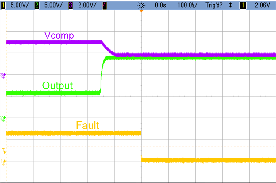 Figure 3-10 Open Load Fault
When the OL condition is triggered with PWM high, the output rises to approximately 14 V due to the TPS92611-Q1 trying to drive 100 mA into infinite impedance. Additionally, the Vcomp drops to low state with the fault triggering low after t(OPEN_deg). Figure 3-11 illustrates when the PWM is pulled low in the open load condition.
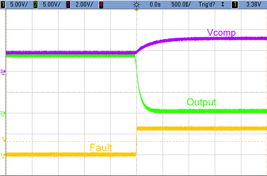 Figure 3-11 Open Load Condition When PWM is Set Low
When the PWM is pulled low during an OL condition, the fault clears immediately. Additionally, the Vcomp returns to a high state with the output dropping to 0 V. Figure 3-12 illustrates device behavior when a SB condition is initially triggered.
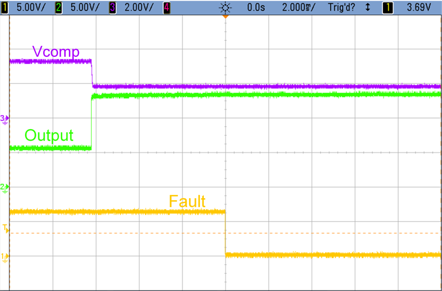 Figure 3-12 Short to Battery Fault Condition
When the SB condition is initially triggered with PWM high, the output increases to the battery voltage (14 V) and Vcomp goes low. Moreover, the fault triggers low following t(OPEN_deg). Figure 3-13 illustrates when the PWM is set low in the SB condition.
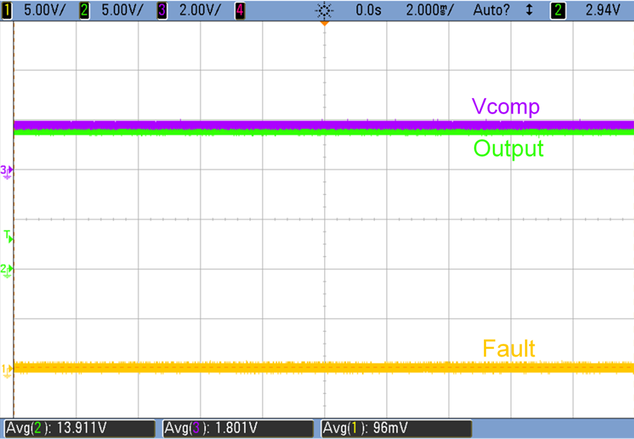 Figure 3-13 Short to Battery Fault When PWM is Set Low
When the PWM is pulled low in the SB condition, nothing changes. Vcomp stays in a high state, the output remains at the supply of 14 V, and the fault remains triggered low. All tests follow Table 3-2 and verify the behavior of the discrete fault detection circuit.