SLVK158A November 2023 – June 2024 TPS7H6003-SP , TPS7H6013-SP , TPS7H6023-SP
PRODUCTION DATA
- 1
- Abstract
- Trademarks
- 1 Introduction
- 2 Single-Event Effects (SEE)
- 3 Device and Test Board Information
- 4 Irradiation Facility and Setup
- 5 Depth, Range, and LETEFF Calculation
- 6 Test Setup and Procedures
- 7 Destructive Single-Event Effects (DSEE)
- 8 Single-Event Transients (SET)
- 9 Event Rate Calculations
- 10Summary
- A References
- B Revision History
3 Device and Test Board Information
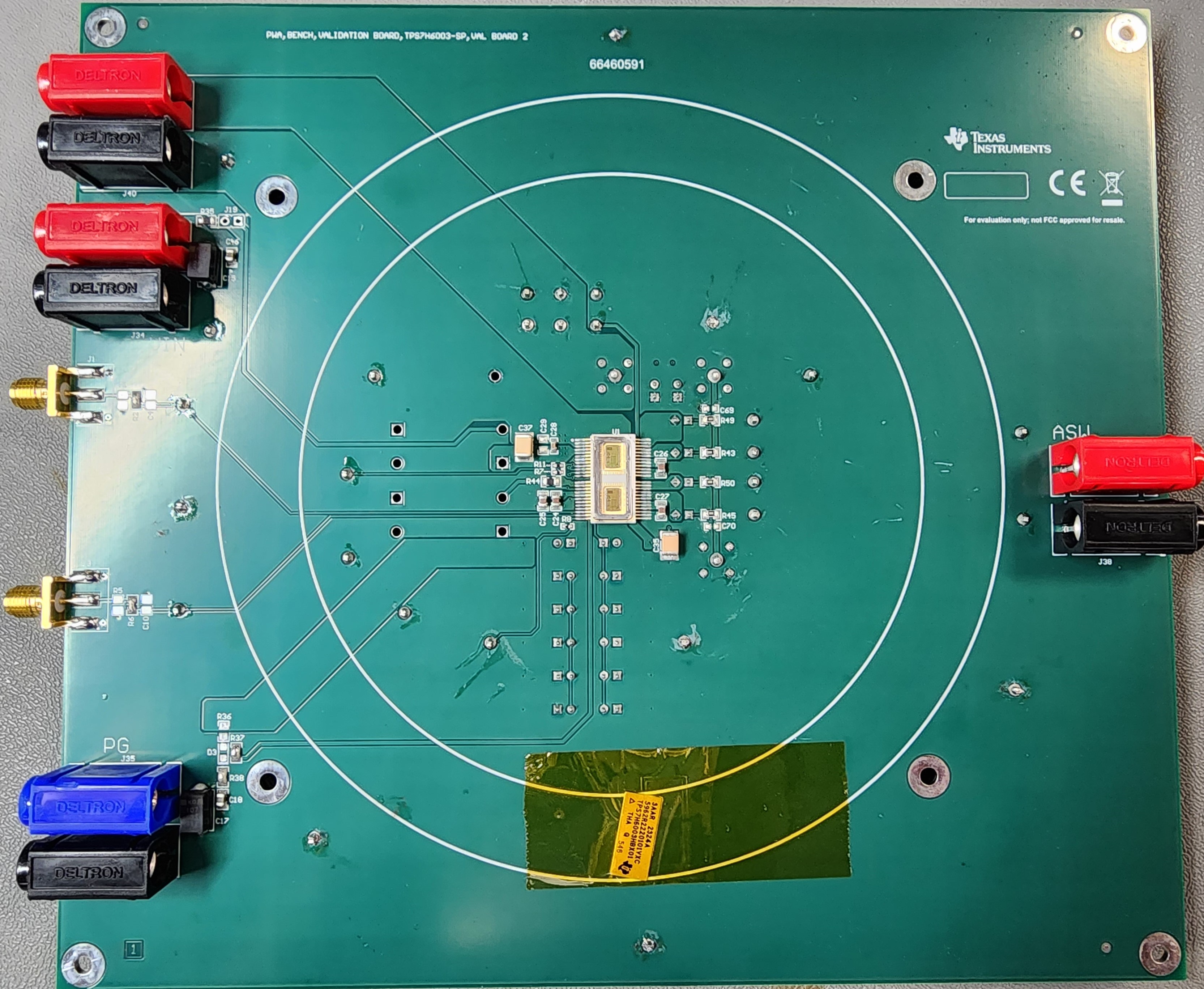
The TPS7H60x3-SP is packaged in a 48-pin ceramic package as shown in Figure 3-1. A TPS7H60X3-SP evaluation board made specifically for radiation testing was used to evaluate the performance and characteristics of the TPS7H60x3-SP under heavy ion radiation. The TPS7H60x3-SP evaluation board is shown in Figure 3-2. The board schematic is shown in Figure 3-3.
The package was delidded to reveal the die face for all heavy-ion testing.
 Figure 3-1 Photograph of Delidded TPS7H6003-SP (Left) and
Pinout Diagram (Right)
 Figure 3-2 TPS7H60X3-SP EVM Top View
Although not shown here, there are 1nF capacitors on the HO and LO outputs. See the block diagram for the setup of the capacitive load.
 Figure 3-3 TPS7H60x3-SP Evaluation Board
Schematics