SLVSAN6B February 2011 – September 2016
PRODUCTION DATA.
- 1 Features
- 2 Applications
- 3 Description
- 4 Revision History
- 5 Device Comparison Table
- 6 Pin Configuration and Functions
- 7 Specifications
- 8 Detailed Description
- 9 Application and Implementation
- 10Power Supply Recommendations
- 11Layout
- 12Device And Documentation Support
- 13Mechanical, Packaging, and Orderable Information
11 Layout
11.1 Layout Guidelines
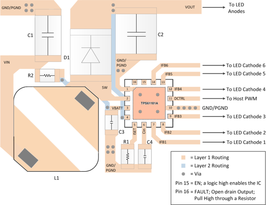
As for all switching power supplies, especially those providing high current and using high switching frequencies, layout is an important design step. If layout is not carefully done, the regulator could show instability as well as EMI problems. Therefore, use wide and short traces for high current paths. The input capacitor, C3 in the typical application circuit, needs not only to be close to the VBAT pin, but also to the GND pin in order to reduce the input ripple detected by the device. The input capacitor, C1 in Figure 9 , must be placed close to the inductor. The SW pin carries high current with fast rising and falling edges. Therefore, keep the connection between the pin to the inductor and Schottky as short and wide as possible. It is also beneficial to have the ground of the output capacitor C2 close to the PGND pin because there is large ground return current flowing between them. When laying out signal ground, TI recommends using short traces separated from power ground traces, connecting these short traces together at a single point, for example on the thermal pad.
Thermal pad must be soldered on to the PCB and connected to the GND pin of the TPS61181A device. Additional thermal via can significantly improve power dissipation of the device.
11.2 Layout Example
 Figure 24. TPS61181A Layout