SLVSD76C February 2016 – July 2017
PRODUCTION DATA.
- 1 Features
- 2 Applications
- 3 Description
- 4 Revision History
- 5 Pin Configuration and Functions
- 6 Specifications
- 7 Parameter Measurement Information
- 8 Detailed Description
- 9 Application and Implementation
- 10Power Supply Recommendations
- 11Layout
- 12Device and Documentation Support
- 13Mechanical, Packaging, and Orderable Information
9 Application and Implementation
NOTE
Information in the following applications sections is not part of the TI component specification, and TI does not warrant its accuracy or completeness. TI’s customers are responsible for determining suitability of components for their purposes. Customers should validate and test their design implementation to confirm system functionality.
9.1 Application Information
This section highlights some of the design considerations when implementing this device in various applications. A PSPICE model for this device is also available in the product page of this device on www.ti.com (See the Device Support section for more information).
9.2 Typical Application
This typical application demonstrates how the TPS22918 can be used to power downstream modules.
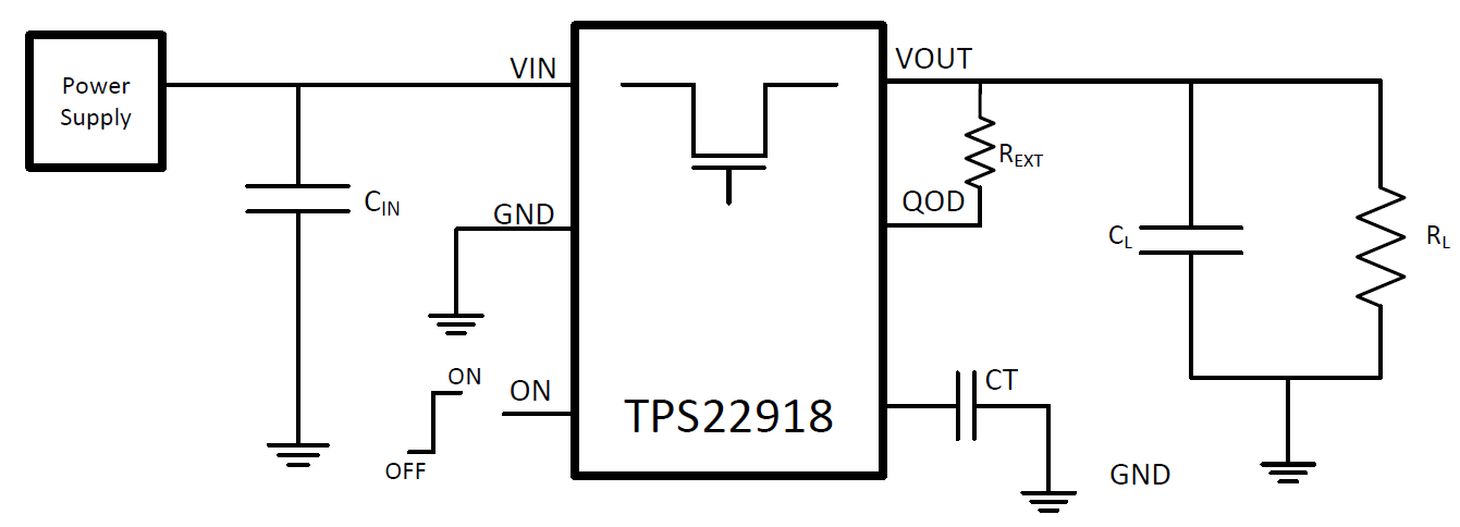 Figure 23. Typical Application Schematic
9.2.1 Design Requirements
For this design example, use the values listed in Table 5 as the design parameters:
Table 5. Design Parameters
| DESIGN PARAMETER | EXAMPLE VALUE |
|---|---|
| VIN | 5 V |
| Load Current | 2 A |
| CL | 22 µF |
| Desired Fall Time | 4 ms |
| Maximum Acceptable Inrush Current | 400 mA |
9.2.2 Detailed Design Procedure
9.2.2.1 Input Capacitor (CIN)
To limit the voltage drop on the input supply caused by transient in-rush currents when the switch turns on into a discharged load capacitor or short-circuit, a capacitor needs to be placed between VIN and GND. A 1 µF ceramic capacitor, CIN, placed close to the pins, is usually sufficient. Higher values of CIN can be used to further reduce the voltage drop during high-current application. When switching heavy loads, it is recommended to have an input capacitor about 10 times higher than the output capacitor to avoid excessive voltage drop.
9.2.2.2 Output Capacitor (CL) (Optional)
Becuase of the integrated body diode in the MOSFET, a CIN greater than CL is highly recommended. A CL greater than CIN can cause VOUT to exceed VIN when the system supply is removed. This could result in current flow through the body diode from VOUT to VIN. A CIN to CL ratio of 10 to 1 is recommended for minimizing VIN dip caused by inrush currents during startup.
9.2.2.3 Shutdown Sequencing During Unexpected System Power Loss
Microcontrollers and processors often have a specific shutdown sequence in which power needs to be removed. Using the adjustable Quick Output Discharge function of the TPS22918, adding a load switch to each power rail can be used to manage the power down sequencing in the event of an unexpected system power loss (i.e. battery removal). To determine the QOD values for each load switch, first confirm the power down order of the device you wish to power sequence. Be sure to check if there are voltage or timing margins that must be maintained during power down. Next, consult QOD Fall Time Table in the Quick Output Discharge (QOD) feature description to determine appropriate COUT and RQOD values for each power rail's load switch so that the load switches' fall times correspond to the order in which they need to be powered down. In the above example, we would like this power rail's fall time to be 4 ms. Using Equation 2, to determine the appropriate RQOD to achieve our desired fall time.
Because fall times are measured from 90% of VOUT to 10% of VOUT, the equation becomes:
Refer to Figure 7, RPD at VIN = 5 V is approximately 25 Ω. Using Equation 1, the required external QOD resistance can be calculated:
Figure 24 through Figure 29 are scope shots demonstrating an example of the QOD functionality when power is removed from the device (both ON and VIN are disconnected simultaneously). The input voltage is decaying in all scope shots below.
- Initial VIN = 3.3 V
- QOD = Open, 500 Ω, or shorted to VOUT
- CL = 1 μF, 10 μF
- VOUT is left floating
NOTE: VIN may appear constant in some figures. This is because the time scale of the scope shot is too small to show the decay of CIN.

| VIN = 3.3 V | CIN = 1 µF | CL = 1 µF |
| QOD = Open | ||
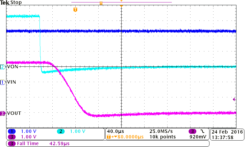
| VIN = 3.3 V | CIN = 1 µF | CL = 1 µF |
| QOD = VOUT | ||
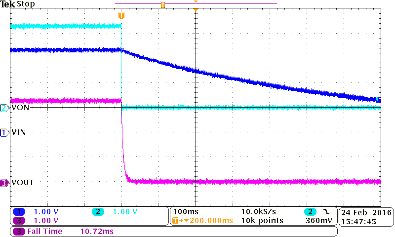
| VIN = 3.3 V | CIN = 1 µF | CL = 10 µF |
| QOD = 500 Ω | ||
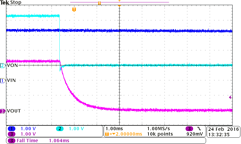
| VIN = 3.3 V | CIN = 1 µF | CL = 1 µF |
| QOD = 500 Ω | ||
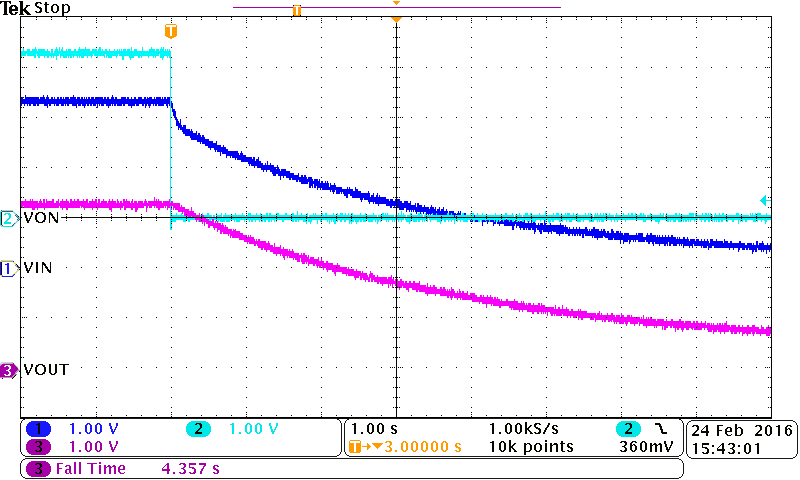
| VIN = 3.3 V | CIN = 1 µF | CL = 10 µF |
| QOD = Open | ||
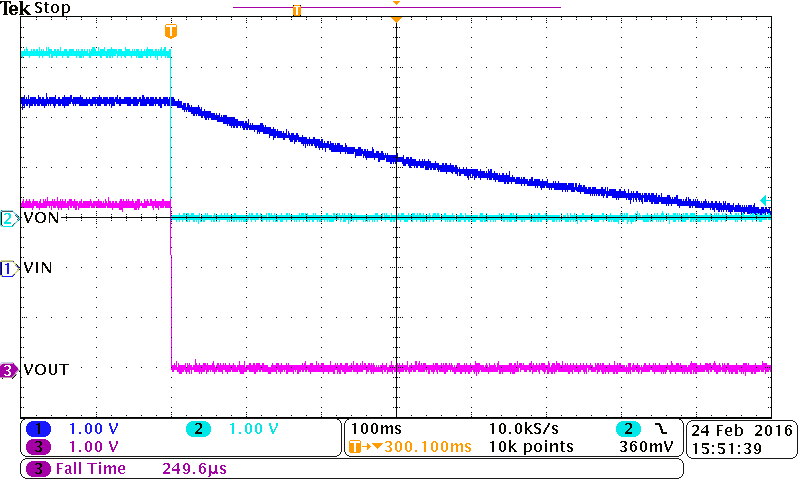
| VIN = 3.3 V | CIN = 1 µF | CL = 10 µF |
| QOD = VOUT | ||
9.2.2.4 VIN to VOUT Voltage Drop
The VIN to VOUT voltage drop in the device is determined by the RON of the device and the load current. The RON of the device depends upon the VIN conditions of the device. Refer to the RON specification of the device in the Electrical Characteristics table of this data sheet. When the RON of the device is determined based upon the VIN conditions, use Equation 8 to calculate the VIN to VOUT voltage drop:
where
- ΔV = voltage drop from VIN to VOUT
- ILOAD = load current
- RON = On-resistance of the device for a specific VIN
9.2.2.5 Inrush Current
Use Equation 9 to determine how much inrush current will be caused by the CL capacitor:

where
- IINRUSH = amount of inrush caused by CL
- CL = capacitance on VOUT
- dt = Output Voltage rise time during the ramp up of VOUT when the device is enabled
- dVOUT = change in VOUT during the ramp up of VOUT when the device is enabled
The appropriate rise time can be calculated using the design requirements and the inrush current equation. As we are calculating the rise time (measured from 10% to 90% of VOUT), we will account for this in our dVOUT parameter (80% of VOUT = 4 V).
To ensure an inrush current of less than 400 mA, choose a CT value that will yield a rise time of more than 220 μs. Consulting Table 2 at VIN = 5 V, CT = 220 pF will provide a typical rise time of 650 μs. Inputting this rise time and voltage into Equation 9, yields:
This inrush current can be seen in the Application Curves section. An appropriate CL value should be placed on VOUT such that the IMAX and IPLS specifications of the device are not violated.
9.2.3 Application Curves
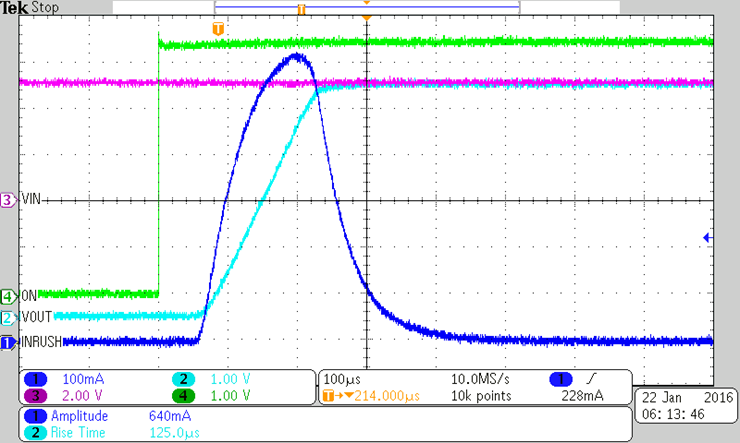
| VIN = 5 V | CL = 22 pF | CT = 0 pF |
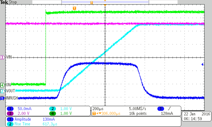
| VIN = 5 V | CL = 22 pF | CT = 220 pF |