SLVU876A February 2013 – May 2021 TPS65279V
5.1 Header Description and Jumper Placement
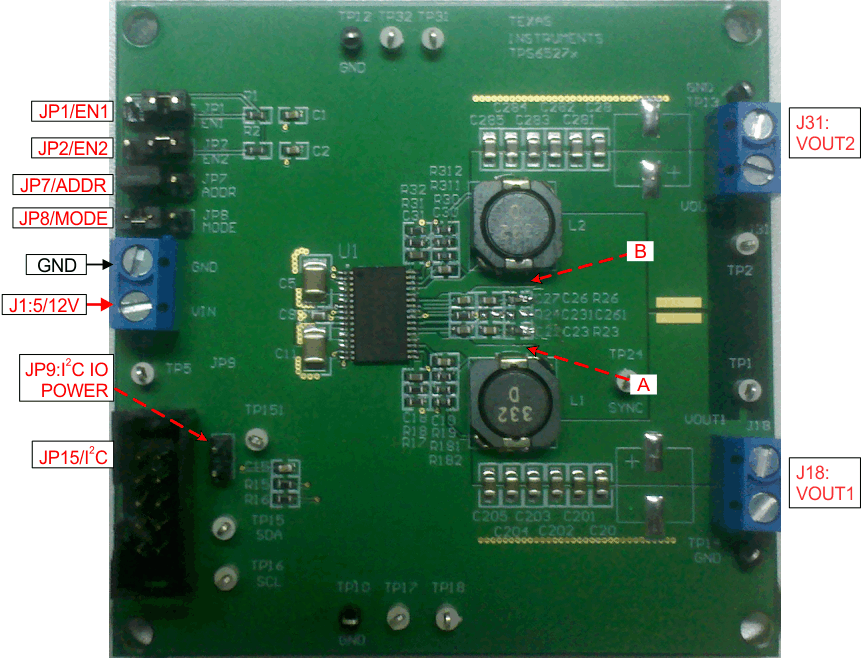
Figure 5-1 illustrates the header description and jumper placement for the EVM.

Test points:
A: LX of Vout1
B: LX of Vout2
Vout1, Vout2
Figure 5-1 Header Description and Jumper PlacementTable 5-1 shows the I/O connections for the EVM.
Table 5-1 Input/Output Connection
| Jumper Number | Function | Description |
|---|---|---|
| J1 | Vin Connector | Apply power supply to this connector |
| J18 | Buck1 Connector | Output of Buck1 |
| J31 | Buck2 Connector | Output of Buck2 |
Table 5-2 shows the jumpers and switches for the EVM.
Table 5-2 Jumpers and Switches
| Jumper Number | Function | Placement | Comment |
|---|---|---|---|
| JP1 | Buck1 enable (EN1) | Connect EN1 to GND to disable Vout1, connect EN1 to Vin through a 100-kΩ resistor to enable Vout1; Leave open to enable Vout1 | |
| JP2 | Buck2 enable (EN2) | Connect EN2 to GND to disable Vout2, connect EN2 to Vin through a 100-kΩ resistor to enable Vout2; Leave open to enable Vout2 | |
| JP7 | I2C address | I2C address configuration pin. Connect this pin to GND to set address 0x60H; connect it to Vcc to set address 0x61H; leave it open to set address 0x62H | On board Vcc is 6.25 V |
| JP8 | Mode | Operation mode control pin. Connect this pin to GND to set forced PWM mode; leave the pin open to set auto PSM-PWM; connect this pin to Vcc set the IC to run in current share mode. | |
| JP9 | I2C Power | Power connected to the I2C IO pull-up resistor; Leave the two pins un-connected set the power to be 3.3V from the I2C interface adaptor; short the two pins set the power to be Vcc. | On board Vcc is 6.25 V |
| JP15 | I2C interface connector | Pin 5 is 3.3 V from adaptor; pin 6 is Ground; pin 9 is SCL, pin 10 is SDA. |