SLVUBI1 May   2021


  1.   Trademarks
  2. 1TPS7H4002EVM-CVAL Overview
    1. 1.1 Features
    2. 1.2 Applications
  3. 2TPS7H4002EVM-CVAL Default Configuration
  4. 3TPS7H4002EVM-CVAL Initial Setup
  5. 4TPS7H4002EVM-CVAL Testing
    1. 4.1 Output Voltage Regulation
    2. 4.2 Output Voltage Ripple
    3. 4.3 Soft Start-up
    4. 4.4 Transient Response to Positive/Negative Load Step (0 A to 3A to 0A)
    5. 4.5 Input Voltage Ripple
    6. 4.6 Loop Frequency Response
    7. 4.7 Current Limiting
  6. 5TPS7H4002EVM-CVAL EVM Schematic
  7. 6TPS7H4002EVM-CVAL Bill of Materials (BOM)
  8. 7Board Layout

Output Voltage Ripple

Display CH1 (PH1) and CH2 (VOUT1) [AC coupled, BW = 20 MHz] on the oscilloscope to monitor the switching phase node and the output voltage ripple as shown in Figure 4-2.
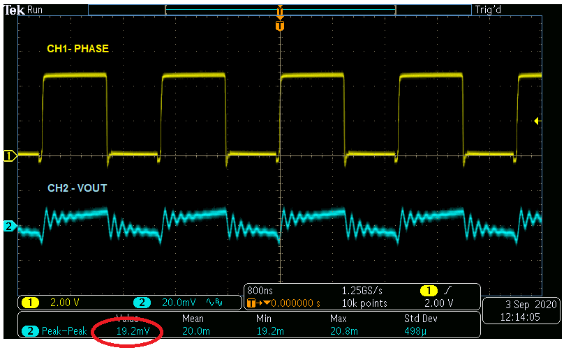
GUID-20210517-CA0I-XP8Z-BPRC-WCMZJ36X4V9J-low.png Figure 4-2 Output Voltage Ripple VIN = 5 V, VOUT = 2.5 V, IOUT = 3 A