SLVUBO3A April 2019 – October 2020 TPS650330-Q1
- Trademarks
- 1BOOSTXL-TPS65033 Components and Environment
- 2BOOSTXL-TPS65033 Board Information
- 3Programming GUI Operation
- 4Recommended Operating Procedure
- 5BOOSTXL-TPS65033 Schematic
- 6BOOSTXL-TPS65033 Board Layers
- 7BOOSTXL-TPS65033 Bill of Materials
- 8Revision History
3.4 Scripting
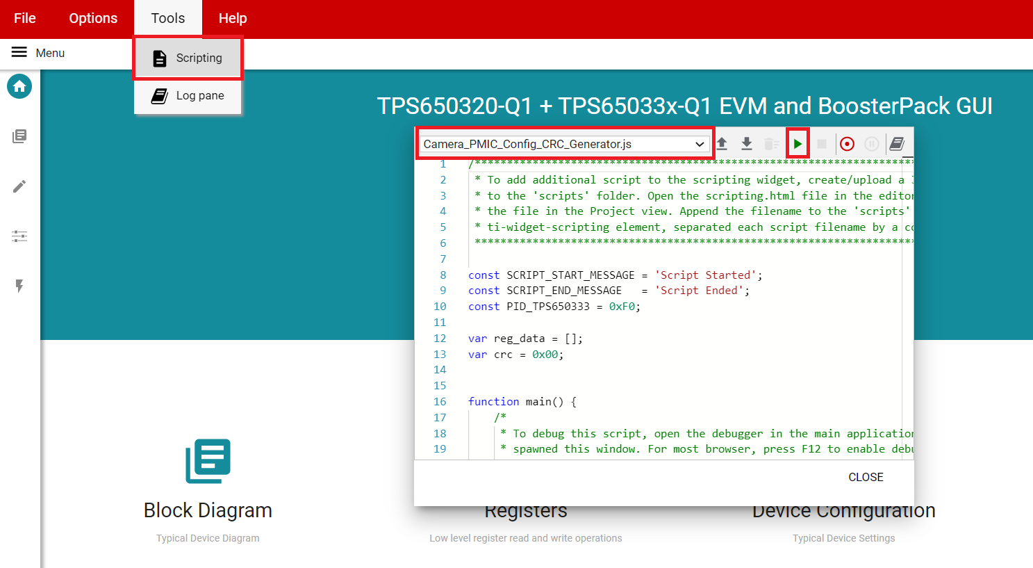
The GUI includes a scripting feature in the tools menu at the top of the window. Scripting enables automated writes and reads to the PMIC, allowing sequential instructions to be sent to the PMIC. Scripts can be saved as a .js or .txt file, and imported using the Upload arrow at the top of the scripting window. Scripting allows the re-configuration of multiple PMICs before sending to assembly or populating on a PCB.
 Figure 3-21 TPS6503xx-Q1 GUI Scripting
Window
Figure 3-21 TPS6503xx-Q1 GUI Scripting
WindowAn example script for re-programming a device can be seen below, where output voltages and sequencing settings are reconfigured from the default settings.
/* Entry point for the script, which will be executed when the user presses the PLAY button in the Scripting Dialog. */
function main() {
write('CONTROL_LOCK', 0xDD);     // Unlock control registers
write('CONFIG_LOCK', 0xAA);      // Unlock configuration registers
write('GPIO_CTRL',2);            // Disable configuration CRC
write('BUCK_LDO_CTRL',0x00);     // Turn off all regulators to prevent faults
write('BUCK3_VOUT',6);           // Change Buck 3 output voltage
write('LDO_VOUT',8);             // Change LDO output voltage
write('SEQ_TRIG_BUCK2',10);      // Update Buck 2 sequence dependencies
write('SEQ_TRIG_BUCK3',2);       // Update Buck 3 sequence dependencies
write('SEQ_TRIG_LDO',26);        // Update LDO sequence dependencies
write('SEQ_TRIG_nRSTOUT',2);     // Update nRSTOUT sequence dependencies
write('BUCK1_SEQ_DLY',145);      // Update Buck 1 sequence delay
write('BUCK2_SEQ_DLY',86);       // Update Buck 2 sequence delay
write('BUCK3_SEQ_DLY',54);       // Update Buck 3 sequence delay
write('LDO_SEQ_DLY',118);        // Update LDO sequence delay
write('nRSTOUT_SEQ_DLY',6);      // Update nRSTOUT sequence delay
write('BUCK_LDO_CTRL',31);       // Re-enable all regulators
write('EEPROM_PROG_CMD',45);     // Burn settings into EEPROM
}
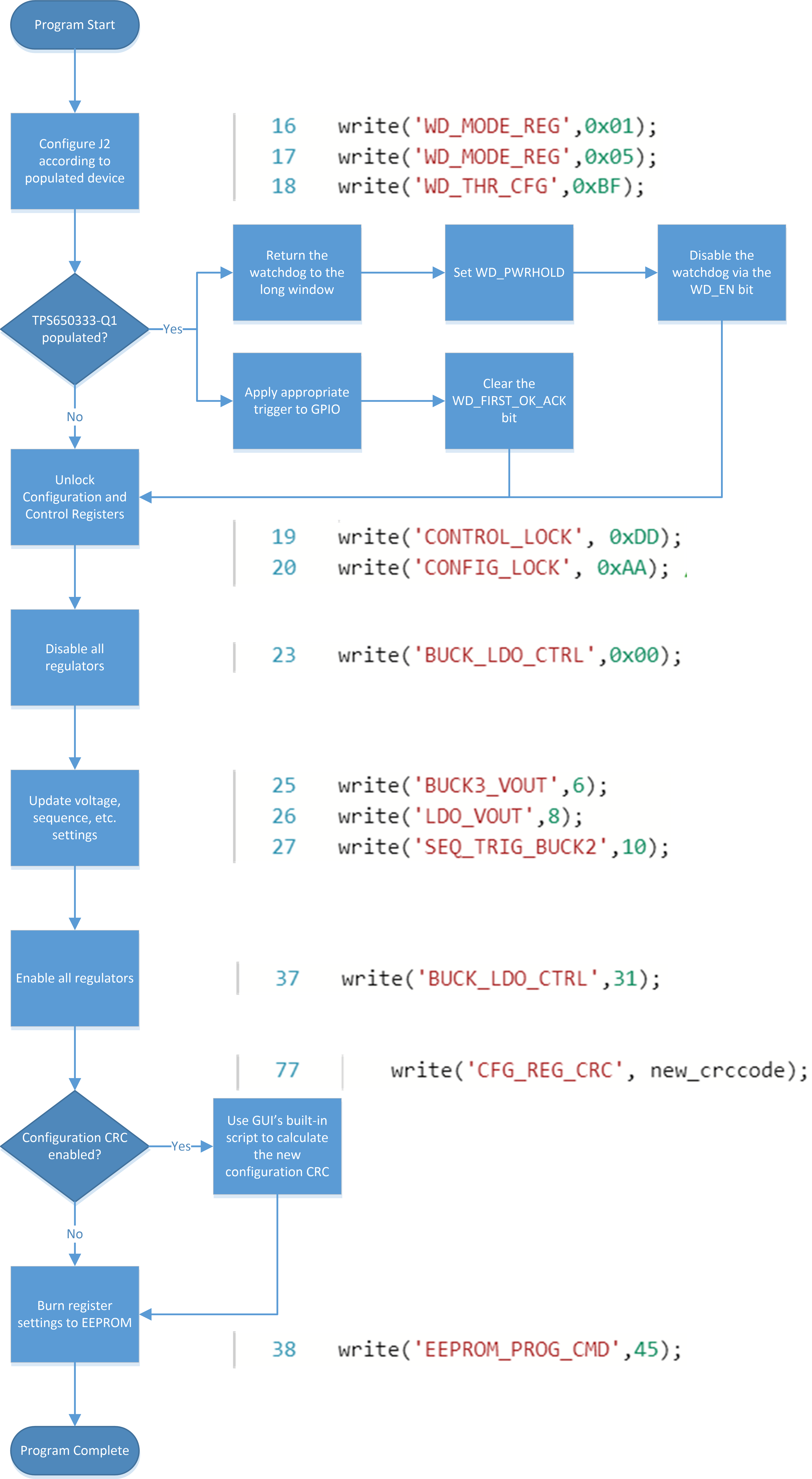
Figure 3-22 details the typical device programming flow. Most blocks can be executed with one or more register write commands in the script file. Only the J2 configuration and GPIO trigger application cannot be done via scripting.
 Figure 3-22 Example Script Program
Flow