SLVUBW5A June   2020  – October 2020


  1.   Trademarks
  2. 1Introduction
    1. 1.1 Performance Specification
    2. 1.2 Modification
  3. 2Connector, Test Point and Jumper Descriptions
    1. 2.1 Connector and Test Point Descriptions
    2. 2.2 Jumper Configuration
      1. 2.2.1 JP1 (ENABLE)
      2. 2.2.2 JP2(SYNC)
  4. 3Test Procedure
  5. 4Schematic, Bill of Materials, and Board Layout
    1. 4.1 Schematic
    2. 4.2 Bill of Materials
    3. 4.3 Board Layout
  6. 5Revision History

Board Layout

Figure 4-2 through Figure 4-5 illustrate the EVM board layouts.
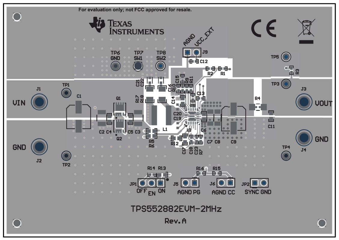
GUID-DFD74121-4DB8-4A54-874C-4B729DDE9BBA-low.gif Figure 4-2 TPS552882EVM-2MHz Top-Side Layout
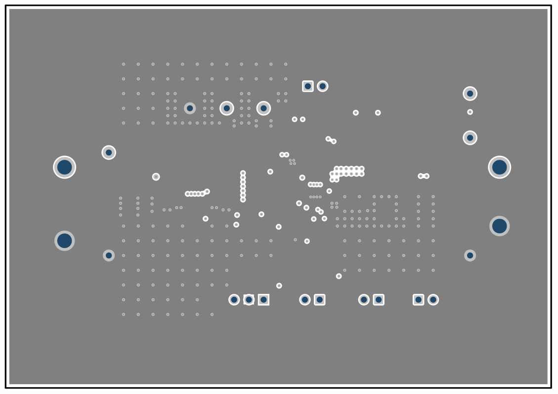
GUID-3A88A28A-4A2A-43E0-B825-0FB28B5B07C0-low.gif Figure 4-3 TPS552882EVM-2MHz Inner Layer1
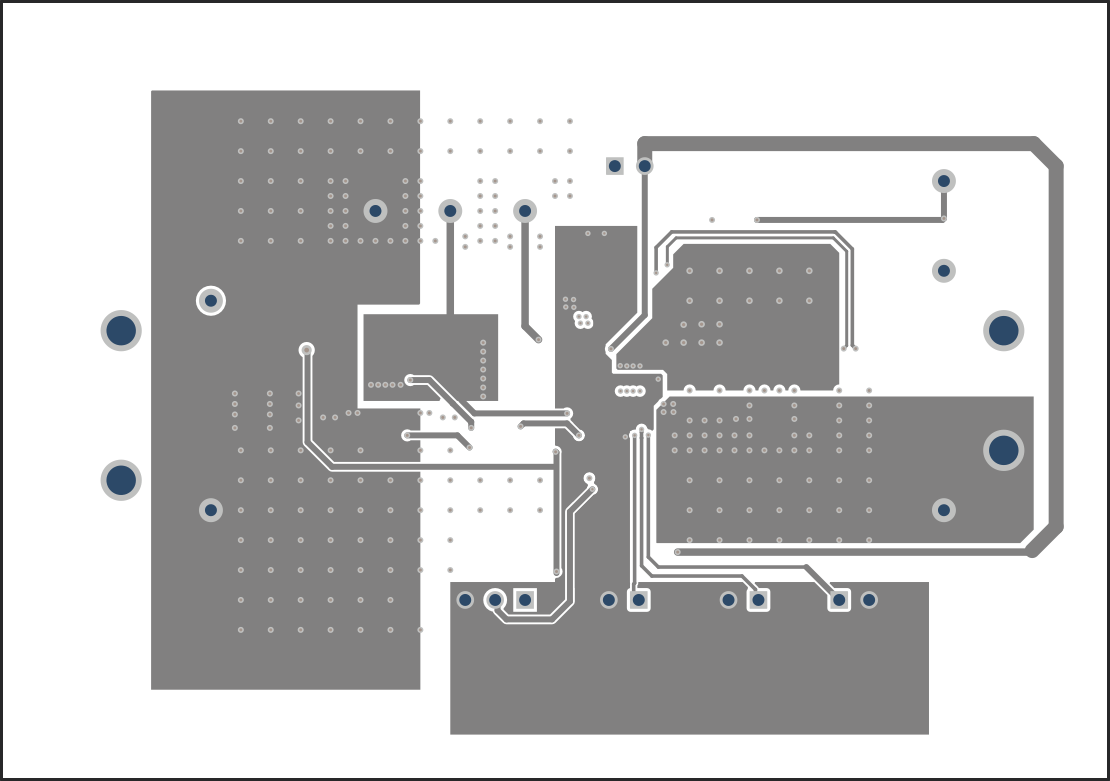
GUID-28628CF8-7DD1-467B-9053-F2F6D5F120B8-low.gif Figure 4-4 TPS552882EVM-2MHz Inner Layer2
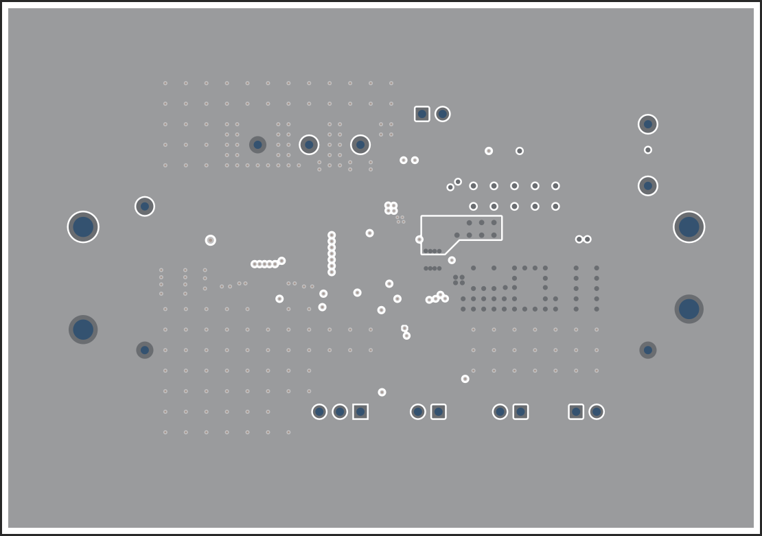
GUID-60155D25-76F5-44B9-BFF9-14A113128B80-low.gif Figure 4-5 TPS552882EVM-2MHz Bottom-Side Layout