SNAS513F August 2011 – November 2015 LM48560
PRODUCTION DATA.
- 1 Features
- 2 Applications
- 3 Description
- 4 Revision History
- 5 Pin Configuration and Functions
- 6 Specifications
- 7 Parameter Measurement Information
- 8 Detailed Description
- 9 Application and Implementation
- 10Power Supply Recommendations
- 11Layout
- 12Device and Documentation Support
- 13Mechanical, Packaging, and Orderable Information
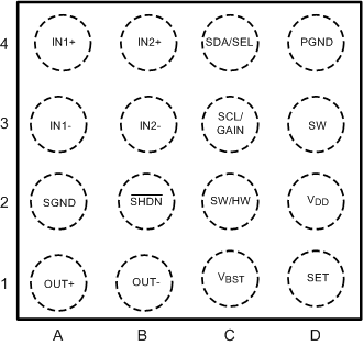
5 Pin Configuration and Functions
YZR Package
16-Pin DSBGA
Top View

Pin Functions
| PIN | I/O | DESCRIPTION | |
|---|---|---|---|
| NO. | NAME | ||
| A1 | OUT+ | O | Amplifier Non-Inverting Output |
| A2 | SGND | — | Amplifier Ground |
| A3 | IN1– | I | Amplifier Inverting Input 1 |
| A4 | IN1+ | I | Amplifier Non-Inverting Input 1 |
| B1 | OUT– | O | Amplifier Inverting Output |
| B2 | SHDN | I | Active Low Shutdown. Connect SHDN to GND to disable device. Connect SHDN to VDD for normal operation |
| B3 | IN2– | I | Amplifier Inverting Input 2 |
| B4 | IN2+ | I | Amplifier Non-Inverting Input 2 |
| C1 | VBST | — | Boost Converter Output |
| C2 | SW/HW | I | Mode Selection Control: SW/HW = 0 → Hardware Mode SW/HW = 1 → Software Mode |
| C3 | SCL/GAIN | I | I2C Serial Clock Input (Software Mode) Gain Select Input (Hardware Mode) see (Table 5) |
| C4 | SDA/SEL | I/O | I2C Serial Data Input (Software Mode) Amplifier Input Select (Hardware Mode) see (Table 5) |
| D1 | SET | — | ALC Timing Input |
| D2 | VDD | — | Power Supply |
| D3 | SW | — | Boost Converter Switching Node |
| D4 | PGND | — | Boost Converter Ground |