SNLA236 September 2015 DS125BR111 , DS125BR401A , DS125BR820
7 Appendix A: Layout Considerations
Storage applications commonly use miniSAS-HD connectors and cages. The 8-channel DS125BR820 can easily fit adjacent to this style of connector to service all eight channels. Two DS125BR820 repeaters can even be placed on opposing sides of the PCB (top and bottom) if that facilitates board routing. The DS125BR820 does not require a heat sink or airflow, since the power consumption is only 70 mW/channel.
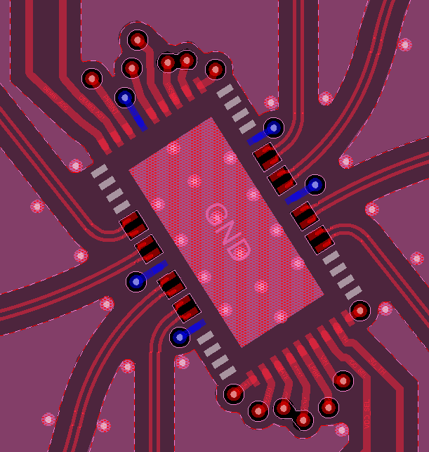
 Figure 13. Evaluation Module Layout Using the DS125BR820
 There are several structures on the evaluation board which aid signal fidelity. In Figure 13 one clear structure is the Reference Plane or GND relief immediately beneath the high speed I/O. By relieving the copper directly under the pads, parasitic capacitance in this area is reduced, helping to bring the local impedance closer to the target value. This is especially true when thin dielectric materials are used to fabricate the outer layers of the PCB.
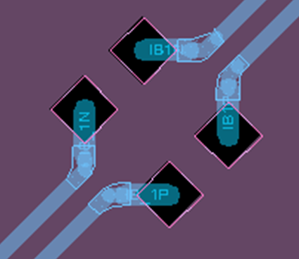
A similar effect can often be detected at AC coupling capacitors when they are placed close to device transmitter outputs. When the extremely small 0201 size SMT capacitors are used, no relief is required. If 0402 size capacitors are used, a relief cutout like the one in Figure 14 is recommended.
 Figure 14. AC Coupling Capacitor Footprint Relief
 The final “structure” is related to the overall differential pair coupling and pair-to-pair spacing. Signals around this type of component are forced into a relatively small space. Fanning signals out to create additional space between pairs will help to control crosstalk levels. Using a differential microstrip with narrow traces and tight coupling in the breakout area immediately around the repeater will also improve the channel isolation in this densely routed space. The evaluation PCB in Table 5 uses a 5-6-5 (w-s-w) differential pair topology to create a 100 Ω signaling environment. The minimum channel-to-channel spacing is 24 mils which results in a 4:1 ratio of inter-pair to intra-pair spacing. For high speed and high loss channels, going below this ratio is not recommended.