SNLA267A March 2019 – June 2019 DS90UB953-Q1 , DS90UB954-Q1 , DS90UB960-Q1
-
How to Design a FPD-Link III System Using DS90UB953-Q1 and DS90UB954-Q1
- Trademarks
- 1 Overview
- 2 Basic Design Rules
- 3 Designing the Link Between SER and DES
- 4 Designing Link Between SER and Image Sensor
- 5 Designing Link Between DES and ISP
- 6 Hardware Design
- 7
Appendix
- 7.1
Scripts
- 7.1.1 BIST Script
- 7.1.2 Example Sensor Initialization Script
- 7.1.3 CSI Enable and Port Forwarding Script
- 7.1.4 Enabling CMLOUT FPD3 RX Port 0 on 954
- 7.1.5 Remote Enabled SER GPIO Toggle Script
- 7.1.6 Local SER GPIO Toggle Script
- 7.1.7 Internal FrameSync on 953 GPIO1
- 7.1.8 External FrameSync on 953 GPIO0
- 7.1.9 SER GPIOs as Inputs and Output to DES GPIO
- 7.1.10 Pattern Generation on the 953 Script
- 7.1.11 Pattern Generation on the 954 Script
- 7.1.12 Monitor Errors for Predetermined Time Script
- 7.1.13 954 and 953 CSI Register Check Script
- 7.1.14 Time Till Lock Script on 953
- 7.2 Acknowledgments
- 7.1
Scripts
- Revision History
4.1 Sensor Initialization Using SER GPIOs
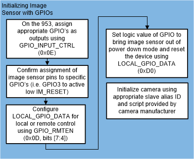
The following steps will generally explain how the initialization of the image sensor occurs from the DS90UB953-Q1. It is important that the link between the SER and DES is working. If the link between the SER and DES is not working, then you will not be able to use the DES to talk to the SER—and subsequently—the image sensor. Example code is listed in Section 7.1.2.
In the example script, the traces on the PCB connect GPIO0 to the imager reset, GPIO1 to the imager power down, GPIO2 to the SER WP, and GPIO3 to frame sync.
- On the serializer enable the appropriate General-Purpose Input/Output (GPIO) pins for output mode.
- On the serializer, GPIO_INPUT_CTRL controls whether GPIO0-3 are configured as inputs or outputs. The first 4 bits [3:0] control whether they are used as inputs, and the last 4 bits [7:4] are used as outputs. Because all GPIOs in this example refer to settings that can be set, all GPIOs are set to outputs. This register has the value of 0x0E.
- GPIO0 and GPIO1 on the 953 can be used for sensing the voltage applied to its input. See Section 6.8 for more information. As a result, GPIO2 and GPIO3 should be used before assigning other GPIO pins.
Table 19. Bit Description of GPIO_INPUT_CTRL Register 0x0E
ADDR. 0x0D[7:4] 0x0D[3:0] Bits XXXX 0000 Desc. Controls if GPIO3-0 are outputs Controls if GPIO3-0 are inputs - Using the serializer, bring to the imager to a known state by bringing the camera out of power-down mode and resetting the camera. This can be accomplished by controlling the GPIO pins.
- On the 953, GPIO0-3 can be locally written to use the LOCAL_GPIO_DATA register. This register can be found at value 0x0D. The last 4 bits [7:4] (GPIO_RMTEN) force the selected GPIO pins to be remotely controlled by the deserializer, which is not required in this example. The concept of remotely controlling GPIOs is discussed in Section 5.1.1.
- Furthermore, the first 4 bits [3:0] (GPIO_OUT_SRC) of the LOCAL_GPIO_DATA register control the logical output of the GPIO registers. Note that the corresponding GPIOs can only be changed when remote enable is disabled and the GPIOs are configured as outputs.
- In the example script, both the imager reset and imager power-down controls are active low. By setting the GPIO1 (IM_PWDN_B) and GPIO2 (SER_WP) to high, the camera is brought out to power-down mode. Then, GPIO0 (IM_RESET) can be held low, which initializes the camera reset. Finally GPIO0 is brought high again to allow initialization of the camera.
- The camera is then initialized by programing the image sensor.
- For example, data can be written to a 32-bit address of the image sensor. This is usually provided by the camera manufacturer. Using ALP, the Python command can be written as:
- Slave_Alias_ID is the I2C alias device ID of the image sensor
- Address_pt1 and Address pt2 make up the address (that is, 0x1234 where Address_pt1 = 0x12 and Address_pt2 = 0x34)
- Data is the data written to that address.
- When the camera has finished initializing, more current will be pulled from the power supply. This will indicate that the camera has successfully initialized. Consider the current limiting setting of the voltage supply. If the total current consumed after initialization is over the current limit of the supply, the voltages in the system will not be regulated correctly.
board.WriteI2C(Slave_Alias_ID, Address_pt1, [Address_pt2,Data])
where:
Table 20. Bit Description of LOCAL_GPIO_DATA Register 0x0D
| ADDR. | 0x0E[7:4] | 0x0E[3:0] |
|---|---|---|
| Bits | 0000 | XXXX |
| Desc. | Enables remote control of SER GPIO3-0 | Controls logical outputs of GPIO3-0 |
