SPRAA99C March 2008 – May 2021 AM3351 , AM3352 , AM3354 , AM3356 , AM3357 , AM3358 , AM3359 , AM4372 , AM4376 , AM4377 , AM4378 , AM4379 , OMAPL138B-EP , TMUX646
2.5 Conventional PCB Design
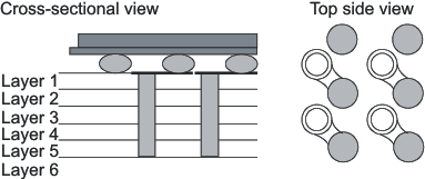
The relatively large via density on the package periphery, mentioned earlier, is caused by limited options when routing the signal from the ball. To reduce or eliminate the via density problem on the periphery of the package, designers can build the PCB vertically from the BGA pad through the internal layers of the board, as shown in Figure 2-6. By working vertically and mechanically drilling 250 μm vias between the pads on the board and the internal layers, designers can create a “pick-and-choose” method. They can pick the layer and choose the route. A “dog bone” method is used to connect the through-hole via and the pad. This reduces the risk of trapped voids that can reduce the board mount process margin.
This method requires a very small mechanical drill to create the necessary number of vias for one package. Although this method is the least expensive, a disadvantage is that the vias go through the board, creating a matrix of vias on the bottom side of the board, which may limit the use of using the back side for routing.
 Figure 2-6 "Dog
Bone" Via Structure