SSZT951 september 2017 AMC1301 , CSD19536KCS , INA240 , TMS320F28033 , UCC21520
In part 1 of this series, I discussed how to integrate bidirectional power flow into your uninterruptible power supply (UPS) designs. In this second installment, I will look more closely at the topology used in the 2kW, 48V to 400V, >93% Efficiency, Isolated Bidirectional DC/DC Converter Reference Design for UPS and battery backup applications.
As I explained in part 1, this reference design works as a voltage-fed full-bridge DC/DC converter while charging the battery, and as an active-clamped current-fed full-bridge converter in backup mode. Achieving high efficiency is very important in backup mode because the maximum power transfer (2kW) takes place in this mode. Let’s look at how the active-clamped current-fed converter works.
While operating in backup mode, the system takes power from a battery, whose voltage can vary from 36V to 60V, and boosts it to an isolated 380V DC bus, which is almost constant. One approach to implement this the boost converter is by using a current-fed converter topology.
Current-fed converters are very good at operating under conditions where either the input or output voltage needs to change over a wide range. They are easy to control, have inherent protection from transformer saturation and are easy to parallel. But traditionally, current-fed converters typically suffer from the drawback that the metal-oxide semiconductor field-effect transistor (MOSFET) experiences high voltage spike at turn-off. Mitigating this drawback necessitates the use of lossy passive snubbers and MOSFETs with higher voltage ratings. For example, a system where the maximum operating input voltage is 60V would require MOSFETs with 150V or 200V. Such high-voltage requirements lead to reduced efficiency because these MOSFETs are not optimized for drain source on-resistance (RDS(on)) and gate charge (Qg).
By adding an active clamp circuit in the low-voltage current-fed full bridge, the reference design reduces the high turn-off voltage spike to less than 15V above the input voltage without additional passive snubbers. The low voltage MOSFET vds during startup is shown in the Figure 1 below.
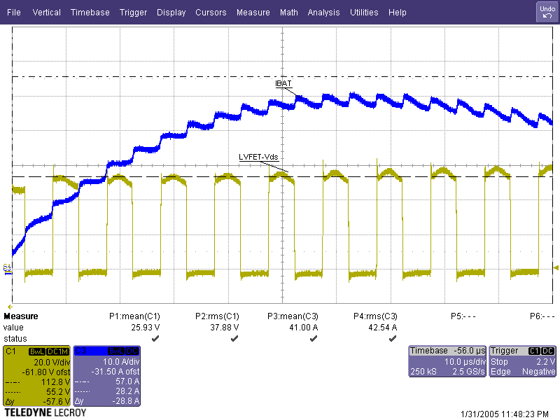 Figure 1 Low Voltage MOSFET Vds vs
Inductor Current at Startup
Figure 1 Low Voltage MOSFET Vds vs
Inductor Current at StartupBy controlling the working of the active clamp circuit, it is possible to use the energy stored in the leakage inductance to achieve zero voltage switching (ZVS) turn-on for the low-voltage MOSFET. This further increases the efficiency of the system in backup mode.
Figure 2 shows the ZVS turn-on of the low-voltage MOSFET. The ZVS range depends on the value of the leakage inductance and the current flowing through the clamp circuit before the active clamp MOSFET turns off.
Current-fed converters have an inherent advantage in that they can ensure zero current switching (ZCS) turn-on of the MOSFET. This is because current-fed converters have overlapped switching periods. For example, before MOSFET pair Q1, Q3 turns on, MOSFET pair Q2, Q4 is already on. This ensures that when Q1 and Q3 are turned-on, the current through them is zero. In the reference design, the low-voltage MOSFETs are always turned on in ZVS or ZCS. See Figure 2 and Figure 3.
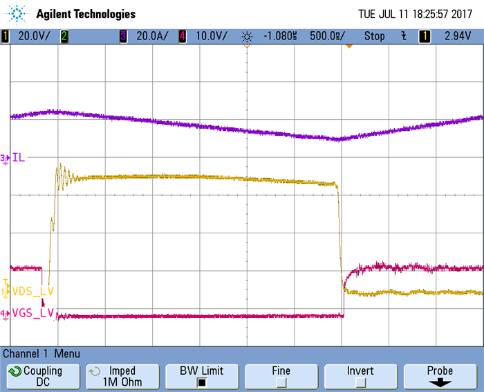 Figure 2 Low Voltage MOSFET Turn on
at ZVS
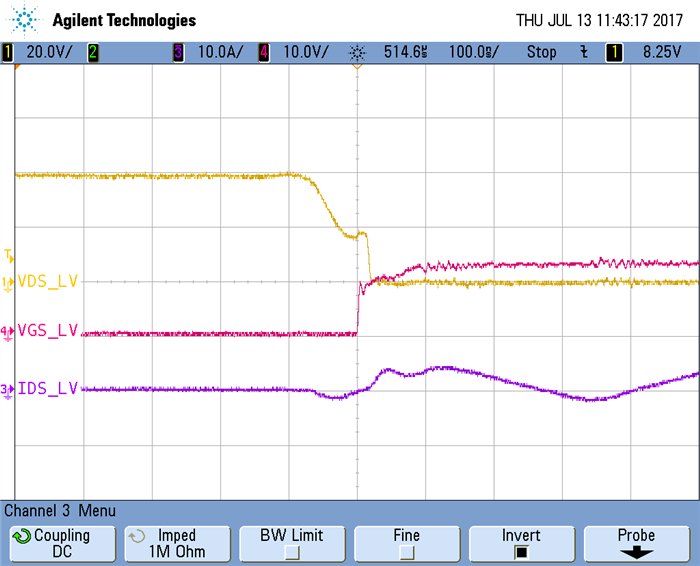 Figure 3 Low Voltage MOSFET Turn on
at ZCS
Figure 3 Low Voltage MOSFET Turn on
at ZCSThe working of the active clamped current fed full bridge and critical waveforms on the primary (low voltage side) are reconstructed in the Figure 4 below. The region marked with the red arrow shows the current transferring into the active clamp when MOSFET pair Q1, Q3 are turned off. This leads to reduced voltage spike on the MOSFET. The region marked in green shows the ZVS turn-on operation.
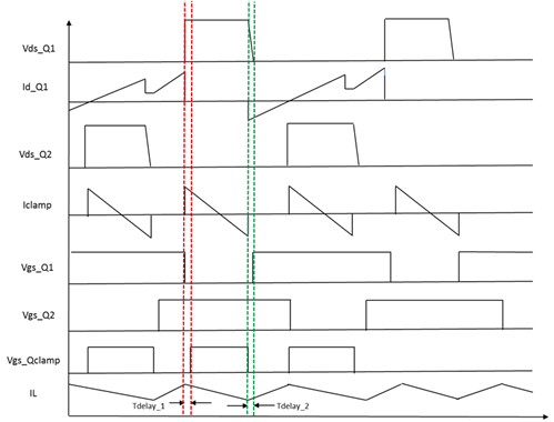
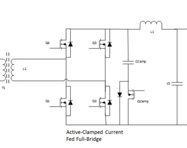 Figure 4 Reconstructed Active Clamped
Current-fed Full Bridge Converter Waveforms
Figure 4 Reconstructed Active Clamped
Current-fed Full Bridge Converter WaveformsCurrent-fed converters ensure ZVS turn-on and turn-off of the high-voltage full-bridge MOSFETs when working as a synchronous rectifier in backup mode. Since this topology works with overlapped switching – where all of the primary low-voltage full-bridge switches are simultaneously on for a short period of time – the di/dt on the secondary-side high-voltage MOSFET at turn off is small, thereby ensuring reduced reverse-recovery losses on the secondary-side MOSFET.
Overall, the use of an active-clamped current-fed converter-based topology shows significant advantages in isolated bidirectional converter applications. The presence of the current-fed inductor smoothens the switching current, hence reducing the ripple current-handling requirements for the input and output capacitors. The advantages it brings in terms of soft-switching capability and ease of control make it a worthwhile candidate for UPS, Battery Backup Unit applications.
Additional Resources
- Discover more reference designs for your next single-phase UPS project.
- Get more insight for your power delivery needs in the TI E2E™ Community.