SSZTA34 June 2017 LM3880-Q1 , TPS51200-Q1 , TPS54116-Q1
Double-data-rate (DDR) memory enables high speed and performance in many electronic systems because of its ability to read and write on both the rising and falling edge of the clock.
The ability to read and write data on both edges of the clock essentially provides two times the speed without increasing clock frequency and enables faster throughput in the system, as the central processing unit (CPU) can more quickly write to and receive data from the DDR.
Automotive subsystems use faster processors and consequently need higher speed and more DDR channels to enable higher performance and a greater user experience in advanced driver assistance systems (ADAS) and vehicle infotainment. Some of the subsystems using DDR include mid- and high-end instrument clusters, touch displays and human machine interface (HMI).
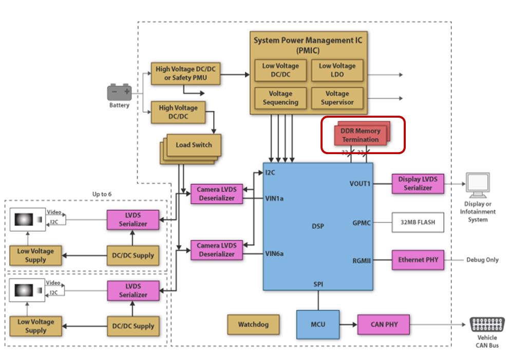
Figure 1 shows a typical surround-view electronic control unit (ECU), including the DDR memory terminator.
 Figure 1 Surround-View ECU
Active DDR termination (typically linear regulators) versus passive termination (resistors) enables lower power dissipation and data integrity. This can make a big difference in the power loss, thermal dissipation and glitch-free performance of a particular subsystem.
DDR memory typically has a core and termination rail, although with DDR4 there is also a third VPP rail (typically 2.5 V) that needs regulating.
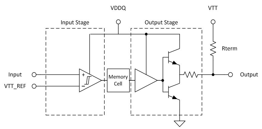
Figure 2 shows a typical DDR memory block diagram.
 Figure 2 DDR Memory Block
Diagram
Figure 2 DDR Memory Block
DiagramDDR memory has half the input-to-output threshold versus conventional memory, low-impedance termination, and terminates to half the input supply. For example, a 1.5-V DDR core rail (VDDQ) requires a 0.75-V DDR termination (VTT).
TI has a complete portfolio of automotive-qualified (Q-100) DDR power solutions, from high-speed linear regulators for termination (DDR VTT rail) to complete DDR core and termination solutions (DDR VDDQ and VTT rail).
The TPS51200-Q1 is a ±3-A source/sink DDR termination low-dropout regulator (LDO) in a 3mm-by-3mm package with fast load transient response and a minimum output capacitance of 20 µF, requiring very small ceramic capacitors. It is compliant with Automotive Electronic Council (AEC)-Q100 test guidance with a -40°C to +125°C ambient operating temperature range, device human body model (HMB) ESD Classification Level 2, and device charged device model (CDM) ESD Classification Level C4B.
The Automotive Off-Battery Processor Power Reference Design for ADAS and Infotainment is one of several automotive designs that includes the TPS51200-Q1.
The TPS54116-Q1 is a full-featured 6-V input 4-A synchronous buck converter for DDR VDDQ and a 1-A source/sink linear regulator for DDR VTT, with a VTTREF buffered reference output. Its 2.5-MHz switching frequency enables very high power density and operation above the medium-wave radio band for enhanced noise immunity.
The Automotive Power Reference Design for Low Power TDA3x-Based Systems includes the TPS54116-Q1, along with the LM3880-Q1 triple rail sequencer.
For your next automotive power subsystem design with DDR memory, consider TI’s large and diverse portfolio of DDR power products, with both linear regulator and switching regulator-based solutions to choose from.