SSZTAL0 November 2016 TL5001 , TPS40170
Buck DC/DC converters (see Figure 1) are a very popular switching DC/DC regulator topology in many electrical and electronic applications, from cloud infrastructure to personal electronics to factory and building automation. They represent >75% of all nonisolated switching regulator topologies today.
The layout of a buck converter is just as important as the simulation and design, but the lack of good layout practices can hamper development time or cause operational and reliability issues down the line.
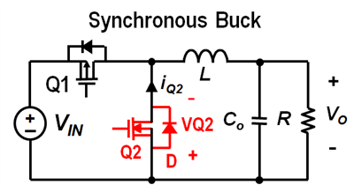 Figure 1 Synchronous Buck DC/DC
Converter
Figure 1 Synchronous Buck DC/DC
ConverterLayout considerations include the placement of bypass capacitors, feedback compensation network components, power components, parasitic components, and ground loops and connections.
Bypass Capacitors
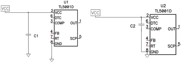 Figure 2 Bypass Capacitor Circuit Connections Indicating Critical Loop Areas
Feedback Compensation Network
 Figure 3 Feedback compensation network placement
Power Components
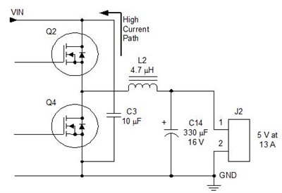 Figure 4 Power Component Connections Indicating a High-current Path
Parasitic Components
Ground Loops and Connections
 Figure 5 Series and Parallel Single-point Ground Connections
A better approach is to use multipoint grounding. As shown in Figure 6, multipoint grounding enables low impedance between circuits to minimize potential differences, and it also reduces circuit trace inductance. The objective is to contain high-frequency currents in individual circuits and keep them out of the ground plane.
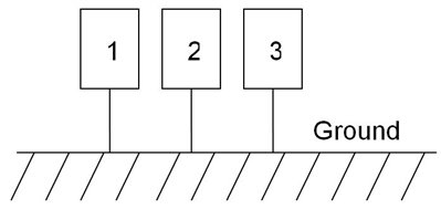 Figure 6 Multipoint Ground Connections
Many buck converter control ICs recognize the noise and quiet circuit areas, and the IC pinout is such that the layout and component placement around the IC pins is easier. Some even provide a separate pin for power and analog ground, as shown in the TPS40170 60V synchronous buck pulse-width modulation (PWM) controller pinout shown in Figure 7.
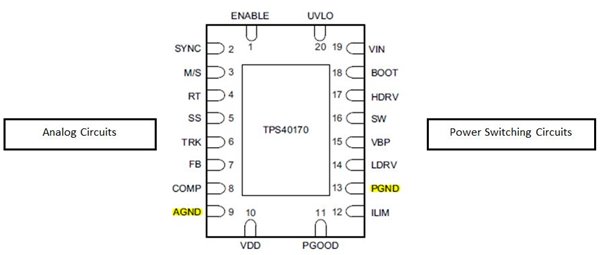 Figure 7 Buck Controller IC Pinout for Analog and Power Connections
So planning for the layout around the IC pinout and using the good layout practices mentioned in this post can help you get your buck converter design working right from the start, and avoid any headaches later. Check out TI’s buck converter and buck controller selection tables for a variety of buck DC/DC solutions.