SSZTB98 may 2016 TPS40041 , TPS40170
The power supply rejection ratio (PSRR) is the power supply’s ability to reject ripple voltage applied at the input. This is normally done by adding a high-current power amplifier in series with the input source, driving it with a frequency-swept signal from a signal analyzer, and measuring the ratio of VIN to VOUT at each measured frequency. These power amplifiers are expensive, however, and easily damaged during testing. In this post, I’ll explain how to dispense with the power amplifier by repurposing a voltage-loop analyzer and making a few low-cost modifications.
Test Setup
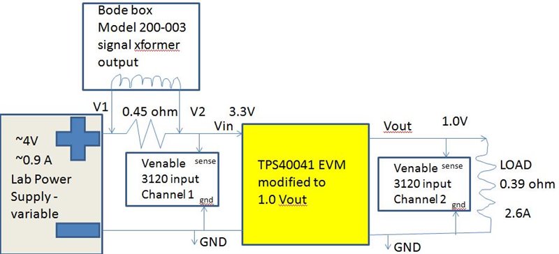
See Figure 1 below: I placed a small resistance in series with the input to apply a frequency-swept AC (Alternating Current) signal at VIN, injected by a signal transformer. The signal is actually applied across the small resistance. I placed three 0.15Ω resistors in series, each rated at 3W, to get 0.45Ω. I adjusted the input to achieve the target 3.3V at the DC/DC (Direct Current to Direct Current) converter input.
 Figure 1 Test Setup
I used a Venable 3120 frequency analyzer with “Bode boxes” and made some modifications.
Typically, the Bode boxes are set up to inject an isolated signal between V1 and V2, and to connect the V1 and V2 signals and ground from the converter under test to the V1 and V2 and ground inputs of the frequency analyzer. This enables one to measure loop gain with only three connections to the converter under test.
Using these same connections for both signal injection and measurement can introduce errors, however, as described in the post, “Power Tips: How connection wires affect Bode plot measurements.” Author Manjing Xie advises using the transformer connections only for injecting signals and having separate connections for measuring V1 and V2.
With PSRR measurements where VOUT is not connected to the injection transformer point, the V2 measurement would in any case need to be separate from the transformer connections. In my test, I injected signals through the Bode box, and had separate connections to measure both V1 (VIN) and V2 (VOUT).
I used the TPS40041 EVM – 001 evaluation module with one modification of R5 from 10k to 30.1k to change VOUT from 1.8V to 1.0V. Switching frequency was at 565-567kHz.
I tested at both no load and 2.6 A load off the 1.0V output.
I used the following generator settings and Bode boxes on the Venable 3120 for the different frequency ranges and took 20 points of data per frequency decade:
- For the 100Hz to 1kHz range I used the 100Hz to 10kHz Bode box (model 200-002) and 1V RMS (Root Mean Square) out of the generator.
- For the 1kHz to 100kHz range I used the 1kHz to 100kHz Bode box (model 200-003) and 1V RMS out of the generator.
- For the 100kHz to 1MHz range I used the 1kHz to 100kHz Bode box (model 200-003) and 10V RMS out of the generator.
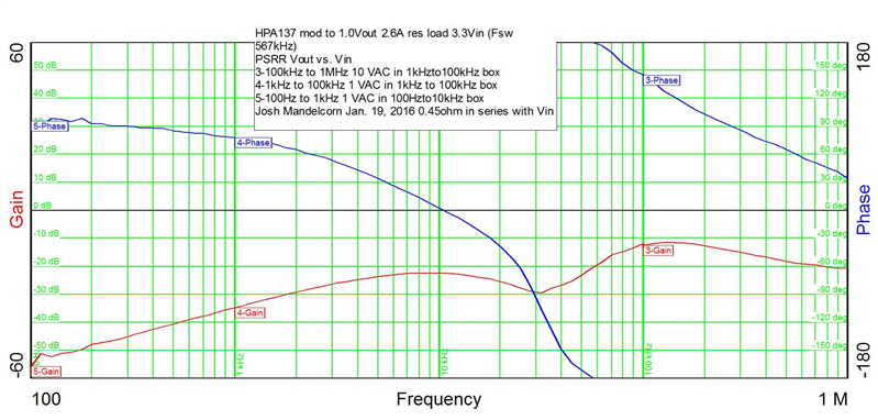
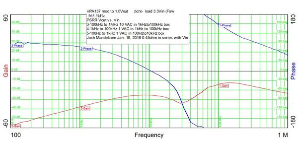
The PSRR results are shown below in Figure 2 for 2.6A load off the 1.0 VOUT and in Figure 3 for no load. The ratio of VOUT/VIN in is shown in red in dB (decibels). The phase relationship is shown in blue in degrees.
 Figure 2 PSRR of Modified TPS40041 EVM at a 2.6A Load
 Figure 3 PSRR of Modified TPS40041 EVM at No Load
Gain and phase patterns are very similar for no load and 2.6A load with attenuation slightly better at no load by about 3 dB at most.
The TPS40041 buck DC/DC controller does not have feed-forward input-voltage compensation in which the pulse-width modulator ramp is proportional to VIN to improve input-voltage rejection. For controllers with feed-forward compensation such as the TPS40170 PWM buck controller, you should expect an even more improved PSRR.
Now you should be able to eliminate the power amplifier by repurposing a voltage-loop analyzer and making a few low-cost modifications. Order the TPS40041 evaluation module or TPS40170 evaluation module and try conducting a similar test yourself.
Additional Resources
- Watch Power Tips videos to help with your design challenges.