SSZTBN6 February 2016 LM53600-Q1 , LM53601-Q1
To ensure that cars meet today’s demand for safety and high reliability, the automotive industry requires original equipment manufacturers (OEMs) to perform 100% automatic visual inspection (AVI) post-assembly. In the case of quad-flat no-lead (QFN) packages, there is no easily viewed solderable or exposed pins/terminals that enable you to determine whether or not the package successfully soldered on to the printed circuit board (PCB). The package edge has exposed copper for the terminals, these are prone to oxidation, making sidewall solder wetting difficult.
With QFN packages, sidewall solder coverage varies from 50-90%. OEMs must incur additional costs due to yield issues from false assembly failures, along with genuine fails where the assembly process has highlighted poor solder joints. The use of an X-ray machine to check for a good, reliable solder joint adds further expense or may not be available.
To resolve the issue of side lead wetting of leadless packaging for automotive and commercial component manufacturers, the wettable flank process was developed. This provides a visual indicator of solderability and lowers the inspection time. TI’s LM53600-Q1 and LM53601-Q1 automotive DC/DC buck regulators are available in a QFN package that uses a wettable flank process approved by many of the largest automotive OEMs.
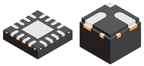
TI adopted special lead plating (SLP) as an additional step during the assembly process, where the package is step-cut and then re-plated with matte tin on half of the sidewall. See Figure 1 and Figure 2.
 Figure 1 Cross-section Comparison
between a Standard QFN and a Sawn-and-plated QFN with Wettable Flanks
 Figure 2 The Partial Cut and Re-plating
of Tin on the Half of the Sidewall of a QFN Package – Section Enlarged on
Right
Figure 2 The Partial Cut and Re-plating
of Tin on the Half of the Sidewall of a QFN Package – Section Enlarged on
RightTin plating provides a protective cover over the exposed copper. During the PCB assembly process, the solder joint will extend from the underside of the pad up the sidewall, resulting in an enhanced solder joint between the component and board. AVI can now assess the presence of a solder joint on all sides of the device. The presence of the side fillet indicates a higher probability of a complete joint, but can't guarantee this inspection at zero parts per million (PPM) without x-ray inspection. Solder de-wetting under the component can still occur due to poor paste block during the printing or PCB land oxidation, and this rate is best estimated as the de-wet PPM of the PCB lands for other non-QFN devices in the same assembly.
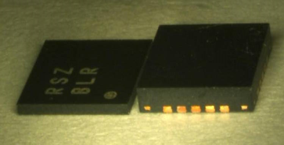
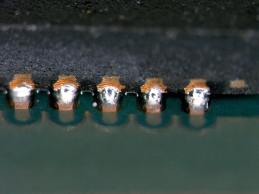
Figure 3 through Figure 6 highlight the solder joint between a QFN lead frame and a PCB with a clear exposed toe fillet, which assists with AVI and removes any false assembly failures.
 Figure 3 Standard QFN Package Side
View
 Figure 4 Toe Fillet on Standard
QFN
 Figure 5 Wettable Flank Lead Frame
Package Sidewall
 Figure 6 Toe Fillet on Wettable Flank
Lead Frame Package QFN
Figure 6 Toe Fillet on Wettable Flank
Lead Frame Package QFNIn summary, you can see that there is no difference in performance or quality with the wettable flank process. In this example, TI’s LM53600-Q1 and LM53601-Q1 automotive DC/DC buck regulators include a reliable solder joint and are able to pass the stringent 100% AVI requirements required by the automotive industry today.