TIDUES6 August 2020 – MONTH
- Description
- Resources
- Features
- Applications
- 5
- 1System Description
- 2System Overview
- 3Hardware, Software, Testing Requirements, and Test Results
- 4Design Files
- 5Software Files
- 6Related Documentation
- 7Terminology
3.2.2.1 Reverse Battery Protection
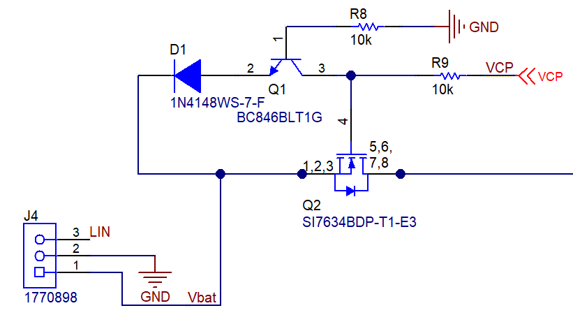
The board is equipped with reverse battery protection. When the power supply is connected properly, current will flow through the reverse battery protection FET (Q2) and onto the rest of the board. The charge pump voltage pin of the DRV8873-Q1 (VCP) provides the high voltage needed to allow current to flow through the FET while the power supply is connected properly. Conversely, when the power supply is connected in reverse, the FET will be off and no current will go to the board. The reverse battery protection circuit is shown in Figure 3-6.
 Figure 3-6 Reverse Battery Protection Circuit
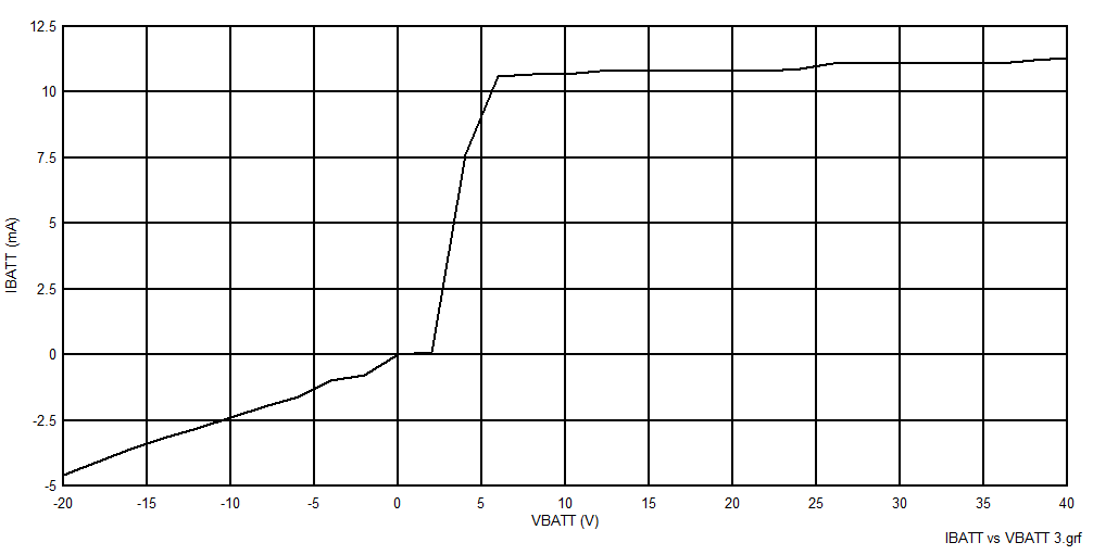
To test the performance of the reverse battery protection circuit, the input voltage was varied from –20 V to 40 V and the input current was measured with a current meter while no loads were being driven. Figure 3-7 shows the input current as a function of the input voltage. At –20 V, the leakage current is close to 5 mA and at 40 V, the input current is around 11 mA.
 Figure 3-7 Input Voltage vs Input Current
Graph