ZHCS155C March 2011 – November 2023 TPS40170
PRODUCTION DATA
- 1
- 1 特性
- 2 应用
- 3 说明
- 4 Pin Configuration and Functions
- 5 Specifications
-
6 Detailed Description
- 6.1 Overview
- 6.2 Functional Block Diagram
- 6.3
Feature Description
- 6.3.1 LDO Linear Regulators and Enable
- 6.3.2 Input Undervoltage Lockout (UVLO)
- 6.3.3 Oscillator and Voltage Feed-Forward
- 6.3.4 Overcurrent Protection and Short-Circuit Protection (OCP and SCP)
- 6.3.5 Soft-Start and Fault-Logic
- 6.3.6 Overtemperature Fault
- 6.3.7 Tracking
- 6.3.8 Adaptive Drivers
- 6.3.9 Start-Up into Pre-Biased Output
- 6.3.10 Power Good (PGOOD)
- 6.3.11 PGND and AGND
- 6.4 Device Functional Modes
-
7 Application and Implementation
- 7.1 Application Information
- 7.2
Typical Application
- 7.2.1 Design Requirements
- 7.2.2
Detailed Design Procedure
- 7.2.2.1 Custom Design with WEBENCH® Tools
- 7.2.2.2 List of Materials
- 7.2.2.3 Select a Switching Frequency
- 7.2.2.4 Inductor Selection (L1)
- 7.2.2.5 Output Capacitor Selection (C9)
- 7.2.2.6 Peak Current Rating of Inductor
- 7.2.2.7 Input Capacitor Selection (C1, C6)
- 7.2.2.8 MOSFET Switch Selection (Q1, Q2)
- 7.2.2.9 Timing Resistor (R7)
- 7.2.2.10 UVLO Programming Resistors (R2, R6)
- 7.2.2.11 Boot-Strap Capacitor (C7)
- 7.2.2.12 VIN Bypass Capacitor (C18)
- 7.2.2.13 VBP Bypass Capacitor (C19)
- 7.2.2.14 VDD Bypass Capacitor (C16)
- 7.2.2.15 SS Timing Capacitor (C15)
- 7.2.2.16 ILIM Resistor (R9, C17)
- 7.2.2.17 SCP Multiplier Selection (R5)
- 7.2.2.18 Feedback Divider (R10, R11)
- 7.2.2.19 Compensation: (R4, R13, C13, C14, C21)
- 7.2.3 Application Curves
- 7.3 Power Supply Recommendations
- 7.4 Layout
- 8 Device and Documentation Support
- 9 Revision History
- 10Mechanical, Packaging, and Orderable Information
6.3.1 LDO Linear Regulators and Enable
The TPS40170 has two internal low-drop-out (LDO) linear regulators. One has a nominal output voltage of VVBP and is present at the VBP pin. This is the voltage that is mainly used for the gate-driver output. The other linear regulator has an output voltage of VVDD and is present at the VDD pin. This voltage can be used in external low-current logic circuitry. The maximum allowable current drawn from the VDD pin must not exceed 5 mA.
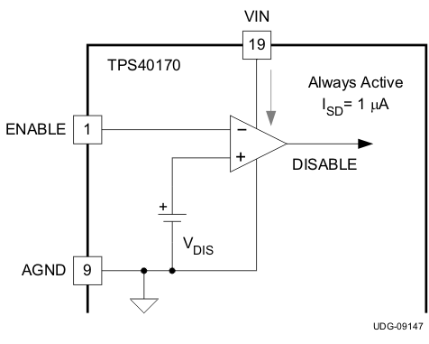
The TPS40170 has a dedicated device enable pin (ENABLE). This simplifies user level interface design because no multiplexed functions exist. If the ENABLE pin of the TPS40170 is higher than VEN, then the LDO regulators are enabled. To ensure that the LDO regulators are disabled, the ENABLE pin must be pulled below VDIS. By pulling the ENABLE pin below VDIS, the device is completely disabled and the current consumption is very low (nominally, 1 µA). Both LDO regulators are actively discharged when the ENABLE pin is pulled below VDIS. A functionally equivalent circuit to the enable circuitry on the TPS40170 is shown in Figure 6-1.
 Figure 6-1 TPS40170 Enable Functional Block
The ENABLE pin must not be allowed to float. If the ENABLE function is not needed for the design, then it is suggested that the ENABLE pin be pulled up to VIN by a high value resistor ensuring that the current into the ENABLE pin does not exceed 10 µA. If it is not possible to meet this clamp current requirement, then it is suggested that a resistor divider from VIN to GND be used to connect to ENABLE pin. The resistor divider must be such that the ENABLE pin must be higher than VEN and lower than 8 V.
To avoid potential erroneous behavior of the enable function, the ENABLE signal applied must have a minimum slew rate of 20 V/s.