ZHCS179F August 2011 – July 2016
PRODUCTION DATA.
- 1 特性
- 2 应用
- 3 说明
- 4 修订历史记录
- 5 Device Comparison Table
- 6 Pin Configuration and Functions
- 7 Specifications
-
8 Detailed Description
- 8.1 Overview
- 8.2 Functional Block Diagram
- 8.3 Feature Description
- 8.4 Device Functional Modes
- 9 Application and Implementation
- 10Power Supply Recommendations
- 11Layout
- 12器件和文档支持
- 13机械、封装和可订购信息
8 Detailed Description
8.1 Overview
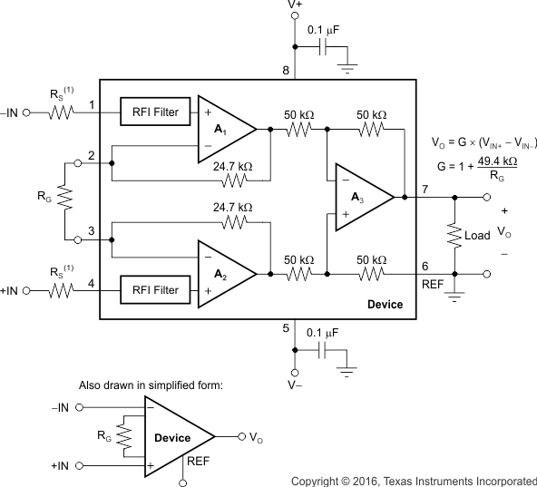
The Functional Block Diagram section shows the basic connections required for operation of the INA826. Good layout practice mandates the use of bypass capacitors placed as close to the device pins as possible.
The output of the INA826 is referred to the output reference (REF) terminal, which is normally grounded. This connection must be low-impedance to assure good common-mode rejection. Although 5 Ω or less of stray resistance can be tolerated when maintaining specified CMRR, small stray resistances of tens of ohms in series with the REF pin can cause noticeable degradation in CMRR.
8.2 Functional Block Diagram
8.3 Feature Description
8.3.1 Inside the INA826
See the Functional Block Diagram section for a simplified representation of the INA826. A more detailed diagram (shown in Figure 58) provides additional insight into the INA826 operation.
Each input is protected by two field-effect transistors (FETs) that provide a low series resistance under normal signal conditions, and preserve excellent noise performance. When excessive voltage is applied, these transistors limit input current to approximately 8 mA.
The differential input voltage is buffered by Q1 and Q2 and is impressed across RG, causing a signal current to flow through RG, R1, and R2. The output difference amplifier, A3, removes the common-mode component of the input signal and refers the output signal to the REF terminal.
The equations shown in Figure 58 describe the output voltages of A1 and A2. The VBE and voltage drop across R1 and R2 produce output voltages on A1 and A2 that are approximately 0.8 V higher than the input voltages.
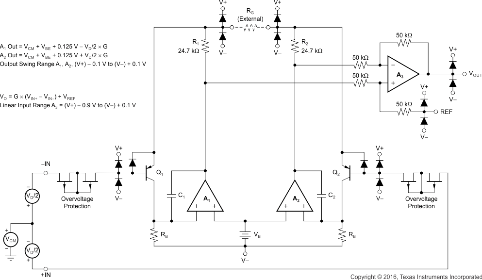 Figure 58. INA826 Simplified Circuit Diagram
8.3.2 Setting the Gain
Gain of the INA826 is set by a single external resistor, RG, connected between pins 2 and 3. The value of RG is selected according to Equation 1:

Table 1 lists several commonly-used gains and resistor values. The 49.4-kΩ term in Equation 1 comes from the sum of the two internal 24.7-kΩ feedback resistors. These on-chip resistors are laser-trimmed to accurate absolute values. The accuracy and temperature coefficients of these resistors are included in the gain accuracy and drift specifications of the INA826.
Table 1. Commonly-Used Gains and Resistor Values
| DESIRED GAIN (V/V) | RG (Ω) | NEAREST 1% RG (Ω) |
|---|---|---|
| 1 | — | — |
| 2 | 49.4 k | 49.9 k |
| 5 | 12.35 k | 12.4 k |
| 10 | 5.489 k | 5.49 k |
| 20 | 2.600 k | 2.61 k |
| 50 | 1.008 k | 1 k |
| 100 | 499 | 499 |
| 200 | 248 | 249 |
| 500 | 99 | 100 |
| 1000 | 49.5 | 49.9 |
8.3.2.1 Gain Drift
The stability and temperature drift of the external gain setting resistor, RG, also affects gain. The contribution of RG to gain accuracy and drift can be directly inferred from the gain of Equation 1.
The best gain drift of 1 ppm/℃ can be achieved when the INA826 uses G = 1 without RG connected. In this case, the gain drift is limited only by the slight mismatch of the temperature coefficient of the integrated 50-kΩ resistors in the differential amplifier (A3). At G greater than 1, the gain drift increases as a result of the individual drift of the 24.7-kΩ resistors in the feedback of A1 and A2, relative to the drift of the external gain resistor RG. Process improvements of the temperature coefficient of the feedback resistors now make possible specifying a maximum gain drift of the feedback resistors of 35 ppm/℃, thus significantly improving the overall temperature stability of applications using gains greater than 1.
Low resistor values required for high gain can make wiring resistance important. Sockets add to the wiring resistance and contribute additional gain error (such as a possible unstable gain error) at gains of approximately 100 or greater. To ensure stability, avoid parasitic capacitance of more than a few picofarads at RG connections. Careful matching of any parasitics on both RG pins maintains optimal CMRR over frequency; see the Typical Characteristics curves (Figure 19 and Figure 20).
8.3.3 Offset Trimming
Most applications require no external offset adjustment; however, if necessary, adjustments can be made by applying a voltage to the REF terminal. Figure 59 shows an optional circuit for trimming the output offset voltage. The voltage applied to the REF terminal is summed at the output. The op amp buffer provides low impedance at the REF terminal to preserve good common-mode rejection.
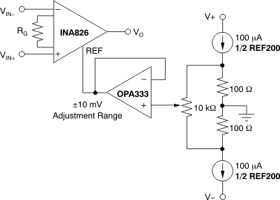 Figure 59. Optional Trimming of the Output Offset Voltage
8.3.4 Input Common-Mode Range
The linear input voltage range of the INA826 input circuitry extends from the negative supply voltage to 1 V below the positive supply and maintains 84-dB (minimum) common-mode rejection throughout this range. The common-mode range for most common operating conditions is described in the input common-mode voltage versus output voltage Typical Characteristics curves (Figure 9 through Figure 15) and the offset voltage versus common-mode voltage curves (Figure 41 through Figure 43). The INA826 can operate over a wide range of power supplies and VREF configurations, thus providing a comprehensive guide to common-mode range limits for all possible conditions is impractical.
The most commonly overlooked overload condition occurs when a circuit exceeds the output swing of A1 and A2, which are internal circuit nodes that cannot be measured. Calculating the expected voltages at the output of A1 and A2 (see Figure 58) provides a check for the most common overload conditions. The designs of A1 and A2 are identical and the outputs can swing to within approximately 100 mV of the power-supply rails. For example, when the A2 output is saturated, A1 can still be in linear operation, responding to changes in the noninverting input voltage. This difference can give the appearance of linear operation but the output voltage is invalid.
A single-supply instrumentation amplifier has special design considerations. To achieve a common-mode range that extends to single-supply ground, the INA826 employs a current-feedback topology with PNP input transistors; see Figure 58. The matched PNP transistors Q1 and Q2 shift the input voltages of both inputs up by a diode drop, and (through the feedback network) shift the output of A1 and A2 by approximately 0.8 V. With both inputs and VREF at single-supply ground (negative power supply), the output of A1 and A2 is well within the linear range, allowing differential measurements to be made at the GND level. As a result of this input level-shifting, the voltages at pin 2 and pin 3 are not equal to the respective input terminal voltages (pin 1 and pin 4). For most applications, this inequality is not important because only the gain-setting resistor connects to these pins.
8.3.5 Input Protection
The inputs of the INA826 are individually protected for voltages up to ±40 V. For example, a condition of –40 V on one input and 40 V on the other input does not cause damage. However, if the input voltage exceeds (V–) – 2 V and the signal source current drive capability exceeds 3.5 mA, the output voltage switches to the opposite polarity; see Figure 17. This polarity reversal can easily be avoided by adding resistance of 10 kΩ in series with both inputs.
Internal circuitry on each input provides low series impedance under normal signal conditions. If the input is overloaded, the protection circuitry limits the input current to a safe value of approximately 8 mA. Figure 17 and Figure 18 illustrate this input current limit behavior. The inputs are protected even if the power supplies are disconnected or turned off.
8.3.6 Input Bias Current Return Path
The input impedance of the INA826 is extremely high—approximately 20 GΩ. However, a path must be provided for the input bias current of both inputs. This input bias current is typically 35 nA. High input impedance means that this input bias current changes very little with varying input voltage.
Input circuitry must provide a path for this input bias current for proper operation. Figure 60 shows various provisions for an input bias current path. Without a bias current path, the inputs float to a potential that exceeds the common-mode range of the INA826 and the input amplifiers saturate. If the differential source resistance is low, the bias current return path can be connected to one input (as shown in the thermocouple example in Figure 60). With higher source impedance, using two equal resistors provides a balanced input with possible advantages of lower input offset voltage as a result of bias current and better high-frequency common-mode rejection.
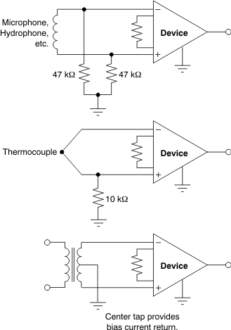 Figure 60. Providing an Input Common-Mode Current Path
8.3.7 Reference Terminal
The output voltage of the INA826 is developed with respect to the voltage on the reference terminal. Often, in dual-supply operation, the reference pin (pin 6) is connected to the low-impedance system ground. In single-supply operation, offsetting the output signal to a precise mid-supply level can be useful (for example, 2.5 V in a 5-V supply environment). To accomplish this level shift, a voltage source can be tied to the REF pin to level-shift the output so that the INA826 can drive a single-supply ADC, for example.
For the best performance, keep the source impedance to the REF terminal below 5 Ω. As illustrated in the Functional Block Diagram section, the reference resistor is at one end of a 50-kΩ resistor. Additional impedance at the REF pin adds to this 50-kΩ resistor. The imbalance in the resistor ratios results in degraded common-mode rejection ratio (CMRR).
Figure 61 shows two different methods of driving the reference pin with low impedance. The OPA330 is a low-power, chopper-stabilized amplifier and therefore offers excellent stability over temperature. The OPA330 is available in the space-saving SC70 and even smaller chip-scale package. The REF3225 is a precision reference in the small SOT23-6 package.
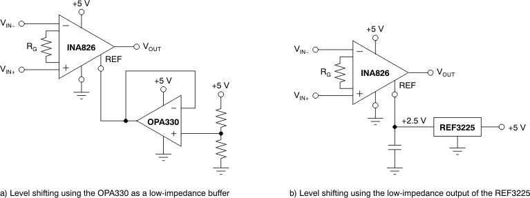 Figure 61. Options for Low-Impedance Level Shifting
8.3.8 Dynamic Performance
Figure 23 illustrates that, despite its low quiescent current of only 200 µA, the INA826 achieves much wider bandwidth than other INAs in its class. This achievement is a result of using TI’s proprietary high-speed precision bipolar process technology. The current-feedback topology provides the INA826 with wide bandwidth even at high gains. Settling time also remains excellent at high gain because of a high slew rate of 1 V/µs.
8.3.9 Operating Voltage
The INA826 operates over a power-supply range of 3 V to 36 V (±1.5 V to ±18 V). Supply voltages higher than 40 V (±20 V) can permanently damage the device. Parameters that vary over supply voltage or temperature are shown in the Typical Characteristics section of this data sheet.
8.3.9.1 Low-Voltage Operation
The INA826 can operate on power supplies as low as ±1.5 V. Most parameters vary only slightly throughout this supply voltage range; see the Typical Characteristics section. Operation at very low supply voltage requires careful attention to assure that the input voltages remain within the linear range. Voltage swing requirements of internal nodes limit the input common-mode range with low power-supply voltage. The Typical Characteristics curves Figure 9 through Figure 15 and Figure 41 through Figure 43 describe the range of linear operation for various supply voltages, reference connections, and gains.
8.3.10 Error Sources
Most modern signal-conditioning systems calibrate errors at room temperature. However, calibration of errors that result from a change in temperature is normally difficult and costly. Therefore, minimizing these errors is important by choosing high-precision components such as the INA826 that have improved specifications in critical areas that impact the precision of the overall system. Figure 62 shows an example application.
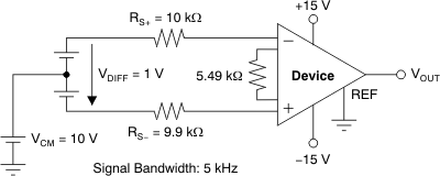 Figure 62. Example Application with G = 10 V/V and 1-V Differential Voltage
Resistor-adjustable INAs such as the INA826 show the lowest gain error in G = 1 because of the inherently well-matched drift of the internal resistors of the differential amplifier. At gains greater than 1 (for instance, G = 10 V/V or G = 100 V/V) the gain error becomes a significant error source because of the contribution of the resistor drift of the 24.7-kΩ feedback resistors in conjunction with the external gain resistor. Except for very high gain applications, the gain drift is by far the largest error contributor compared to other drift errors, such as offset drift.
The INA826 offers excellent gain error over temperature for both G > 1 and G = 1 (no external gain resistor). Table 2 summarizes the major error sources in common INA applications and compares the two cases of G = 1 (no external resistor) and G = 10 (5.49-kΩ external resistor). As can be seen in Table 2, although the static errors (absolute accuracy errors) in G = 1 are almost twice as great as compared to G = 10, there are much fewer drift errors because of the much lower gain error drift. In most applications, these static errors can readily be removed during calibration in production. All calculations refer the error to the input for easy comparison and system evaluation.
Table 2. Error Calculation
| ERROR SOURCE | ERROR CALCULATION | INA826 | ||
|---|---|---|---|---|
| SPECIFICATION | G = 10 ERROR (ppm) | G = 1 ERROR (ppm) | ||
| ABSOLUTE ACCURACY AT 25°C | ||||
| Input offset voltage (μV) | VOSI / VDIFF | 150 | 150 | 150 |
| Output offset voltage (μV) | VOSO / (G × VDIFF) | 700 | 70 | 700 |
| Input offset current (nA) | IOS × maximum (RS+, RS–) / VDIFF | 5 | 50 | 50 |
| CMRR (dB) | VCM / (10CMRR/20 × VDIFF) | 104 (G = 10), 84 (G = 1) |
63 | 631 |
| Total absolute accuracy error (ppm) | 333 | 1531 | ||
| DRIFT TO 105°C | ||||
| Gain drift (ppm/°C) | GTC × (TA – 25) | 35 (G = 10), 1 (G = 1) |
2800 | 80 |
| Input offset voltage drift (μV/°C) | (VOSI_TC / VDIFF) × (TA – 25) | 2 | 160 | 160 |
| Output offset voltage drift (μV/°C) | [VOSO_TC / ( G × VDIFF)] × (TA – 25) | 10 | 80 | 800 |
| Offset current drift (pA/°C) | IOS_TC × maximum (RS+, RS–) × (TA – 25) / VDIFF |
60 | 48 | 48 |
| Total drift error (ppm) | 3088 | 1088 | ||
| RESOLUTION | ||||
| Gain nonlinearity (ppm of FS) | 5 | 5 | 5 | |
| Voltage noise (1 kHz) |  |
eNI = 18, eNO = 110 |
10 | 10 |
| Total resolution error (ppm) | 15 | 15 | ||
| TOTAL ERROR | ||||
| Total error | Total error = sum of all error sources | 3436 | 2634 | |
8.4 Device Functional Modes
The INA826 has a single functional mode and is operational when the power-supply voltage is greater than 3 V (±1.5 V). The maximum power-supply voltage for the INA826 is 36 V (±18 V).