ZHCS234B August 2012 – January 2016 PCM5141 , PCM5142
PRODUCTION DATA.
- 1 特性
- 2 应用
- 3 说明
- 4 修订历史记录
- 5 Device Comparison
- 6 Pin Configuration and Functions
-
7 Specifications
- 7.1 Absolute Maximum Ratings
- 7.2 ESD Ratings
- 7.3 Recommended Operating Conditions
- 7.4 Thermal Information
- 7.5 Electrical Characteristics
- 7.6 Timing Requirements: SCK Input
- 7.7 Timing Requirements: PCM Audio Data
- 7.8 Timing Requirements: I2S Master
- 7.9 Timing Requirements: XSMT
- 7.10 Switching Characteristics
- 7.11 Typical Characteristics
-
8 Detailed Description
- 8.1 Overview
- 8.2 Functional Block Diagram
- 8.3
Feature Description
- 8.3.1 Terminology
- 8.3.2 Audio Data Interface
- 8.3.3 XSMT Pin (Soft Mute / Soft Un-Mute)
- 8.3.4 Audio Processing
- 8.3.5 DAC Outputs
- 8.3.6
Reset and System Clock Functions
- 8.3.6.1 Clocking Overview
- 8.3.6.2 Clock Slave Mode With Master and System Clock (SCK) Input (4 Wire I2S)
- 8.3.6.3 Clock Slave Mode With BCK PLL to Generate Internal Clocks (3-Wire PCM)
- 8.3.6.4 Clock Generation Using the PLL
- 8.3.6.5 PLL Calculation
- 8.3.6.6 Clock Master Mode from Audio Rate Master Clock
- 8.3.6.7 Clock Master from a Non-Audio Rate Master Clock
- 8.4 Device Functional Modes
- 8.5 Programming
- 9 Application and Implementation
- 10Power Supply Recommendations
- 11Layout
- 12Register Maps
- 13器件和文档支持
- 14机械、封装和可订购信息
7 Specifications
7.1 Absolute Maximum Ratings
over operating free-air temperature range (unless otherwise noted)| MIN | MAX | UNIT | ||
|---|---|---|---|---|
| Supply voltage | AVDD, CPVDD, DVDD | –0.3 | 3.9 | V |
| LDO with DVDD at 1.8 V | –0.3 | 2.25 | ||
| Digital input voltage | DVDD at 1.8 V | –0.3 | 2.25 | V |
| DVDD at 3.3 V | –0.3 | 3.9 | ||
| Analog input voltage | –0.3 | 3.9 | V | |
| Operating junction temperature, TJ | –40 | 130 | °C | |
| Storage temperature, Tstg | –65 | 150 | °C | |
7.2 ESD Ratings
| VALUE | UNIT | |||
|---|---|---|---|---|
| V(ESD) | Electrostatic discharge | Human-body model (HBM), per ANSI/ESDA/JEDEC JS-001(1) | ±2000 | V |
| Charged-device model (CDM), per JEDEC specification JESD22-C101(2) | ±750 | |||
(1) JEDEC document JEP155 states that 500-V HBM allows safe manufacturing with a standard ESD control process.
(2) JEDEC document JEP157 states that 250-V CDM allows safe manufacturing with a standard ESD control process.
7.3 Recommended Operating Conditions
| MIN | NOM | MAX | UNIT | ||||
|---|---|---|---|---|---|---|---|
| AVDD | Analog power supply voltage | Referenced to AGND(1) | VCOM mode | 3 | 3.3 | 3.46 | V |
| VREF mode | 3.2 | 3.3 | 3.46 | ||||
| DVDD | Digital power supply voltage | Referenced to DGND(1) | 1.8 V DVDD | 1.65 | 1.8 | 1.95 | V |
| 3.3 V DVDD | 3.1 | 3.3 | 3.46 | ||||
| CPVDD | Charge pump supply voltage | Referenced to CPGND(1) | 3.1 | 3.3 | 3.46 | V | |
| MCLK | Master clock frequency | 50 | MHz | ||||
| LOL, LOR | Stereo line output load resistance | 1 | 10 | kΩ | |||
| CLOUT | Digital output load capacitance | 10 | pF | ||||
| TJ | Operating junction temperature | –40 | 130 | °C | |||
(1) All grounds on board are tied together; they must not differ in voltage by more than 0.2-V maximum, for any combination of ground signals.
7.4 Thermal Information
| THERMAL METRIC(1) | PCM512x | UNIT | ||
|---|---|---|---|---|
| RHB (TSSOP) | ||||
| 32 PINS | ||||
| RθJA | Junction-to-ambient thermal resistance | 72.2 | °C/W | |
| RθJC(top) | Junction-to-case(top) thermal resistance | 17.5 | °C/W | |
| RθJB | Junction-to-board thermal resistance | 35.0 | °C/W | |
| ψJT | Junction-to-top characterization parameter | 0.4 | °C/W | |
| ψJB | Junction-to-board characterization parameter | 34.5 | °C/W | |
(1) For more information about trdational and new thermal metrics, see the Semiconductor and IC Package Thermal Metrics application report, SPRA953.
7.5 Electrical Characteristics
TA = 25°C, AVDD = CPVDD = DVDD = 3.3 V, fS = 48 kHz, system clock = 512 fS and 24-bit data (unless otherwise noted).| PARAMETER | TEST CONDITIONS | MIN | TYP | MAX | UNIT | |
|---|---|---|---|---|---|---|
| Resolution | 16 | 24 | 32 | Bits | ||
| DIGITAL INPUT/OUTPUT | ||||||
| Logic Family: 3.3-V LVCMOS Compatible | ||||||
| VIH | Input logic level, high | 0.7 × DVDD | V | |||
| VIL | Input logic level, low | 0.3 × DVDD | V | |||
| IIH | Input logic current, high | VIN = VDD | 10 | µA | ||
| IIL | Input logic current, low | VIN = 0 V | –10 | µA | ||
| VOH | Output logic level, high | IOH = –4 mA | 0.8 × DVDD | V | ||
| VOL | Output logic level, low | IOL = 4 mA | 0.22 × DVDD | V | ||
| Logic Family 1.8-V LVCMOS Compatible | ||||||
| VIH | Input logic level, high | 0.7 × DVDD | V | |||
| VIL | Input logic level, low | 0.3 × DVDD | V | |||
| IIH | Input logic current, high | VIN = VDD | 10 | µA | ||
| IIL | Input logic current, low | VIN = 0 V | –10 | µA | ||
| VOH | Output logic level, high | IOH = –2 mA | 0.8 × DVDD | V | ||
| VOL | Output logic level, low | IOL = 2 mA | 0.22 × DVDD | V | ||
| DYNAMIC PERFORMANCE (PCM MODE)(1)(2) | ||||||
| THD+N at –1 dB(2) | fS = 48 kHz | –93 | –83 | dB | ||
| fS = 96 kHz | –93 | |||||
| fS = 192 kHz | –93 | |||||
| Dynamic range(2) | EIAJ, A-weighted, fS = 48 kHz | 108 | 112 | dB | ||
| EIAJ, A-weighted, fS = 96 kHz | 112 | |||||
| EIAJ, A-weighted, fS = 192 kHz | 112 | |||||
| Signal-to-noise ratio(2) | EIAJ, A-weighted, fS = 48 kHz | 112 | dB | |||
| EIAJ, A-weighted, fS = 96 kHz | 112 | |||||
| EIAJ, A-weighted, fS = 192 kHz | 112 | |||||
| Signal-to-noise ratio with analog mute(2)(3) | EIAJ, A-weighted, fS = 48 kHz | 113 | 123 | dB | ||
| EIAJ, A-weighted, fS = 96 kHz | 113 | 123 | ||||
| EIAJ, A-weighted, fS = 192 kHz | 113 | 123 | ||||
| Channel separation | fS = 48 kHz | 100 / 95 | 109 / 103 | dB | ||
| fS = 96 kHz | 100 / 95 | 109 / 103 | ||||
| fS = 192 kHz | 100 / 95 | 109 / 103 | ||||
| ANALOG OUTPUT | ||||||
| Single-ended output voltage | 2.1 | VRMS | ||||
| Gain error | –6 | ±2.0 | 6 | % of FSR | ||
| Gain mismatch, channel-to-channel | –6 | ±0.5 | 6 | % of FSR | ||
| Load impedance | 5 | kΩ | ||||
| FILTER CHARACTERISTICS–1: NORMAL (8x) | ||||||
| Pass band | 0.45 × fS | kHz | ||||
| Stop band | 0.55 × fS | kHz | ||||
| Stop band attenuation | –60 | dB | ||||
| Pass-band ripple | ±0.02 | dB | ||||
| Delay time | 20 × tS | s | ||||
| FILTER CHARACTERISTICS–2: LOW LATENCY (8x) | ||||||
| Pass band | 0.47 × fS | kHz | ||||
| Stop band | 0.55 × fS | kHz | ||||
| Stop band attenuation | –52 | dB | ||||
| Pass-band ripple | ±0.0001 | dB | ||||
| Delay time | 3.5 × tS | s | ||||
| FILTER CHARACTERISTICS–3: ASYMMETRIC FIR (8x) | ||||||
| Pass band | 0.4 × fS | kHz | ||||
| Stop band | 0.72 × fS | kHz | ||||
| Stop band attenuation | –52 | dB | ||||
| Pass-band ripple | ±0.05 | dB | ||||
| Delay time | 1.2 × tS | s | ||||
| FILTER CHARACTERISTICS–4: HIGH-ATTENUATION (8x) | ||||||
| Pass band | 0.45 × fS | kHz | ||||
| Stop band | 0.45 × fS | kHz | ||||
| Stop band attenuation | –100 | dB | ||||
| Pass-band ripple | ±0.0005 | dB | ||||
| Delay time | 33.7 × tS | s | ||||
| POWER SUPPLY REQUIREMENTS | ||||||
| DVDD | Digital supply voltage | Target DVDD = 1.8 V | 1.65 | 1.8 | 1.95 | VDC |
| DVDD | Digital supply voltage | Target DVDD = 3.3 V | 3 | 3.3 | 3.6 | VDC |
| AVDD | Analog supply voltage | 3 | 3.3 | 3.6 | VDC | |
| CPVDD | Charge-pump supply voltage | 3 | 3.3 | 3.6 | VDC | |
| IDD | DVDD supply current at 1.8 V | fS = 48 kHz, input is bipolar zero data | 11 | 14 | mA | |
| fS = 96 kHz, input is bipolar zero data | 12 | |||||
| fS = 192 kHz, input is bipolar zero data | 14 | |||||
| IDD | DVDD supply current at 1.8 V | fS = 48 kHz, input is 1 kHz – 1 dBFS data | 11 | 14 | mA | |
| fS = 96 kHz, input is 1 kHz – 1 dBFS data | 12 | |||||
| fS = 192 kHz, input is 1 kHz – 1 dBFS data | 14 | |||||
| IDD | DVDD supply current at 1.8 V(4) | fS = N/A, power-down mode | 0.3 | 0.6 | mA | |
| IDD | DVDD supply current at 3.3 V | fS = 48 kHz, input is bipolar zero data | 12 | 15 | mA | |
| fS = 96 kHz, input is bipolar zero data | 13 | |||||
| fS = 192 kHz, input is bipolar zero data | 15 | |||||
| IDD | DVDD supply current at 3.3 V | fS = 48 kHz, input is 1 kHz – 1 dBFS data | 12 | 15 | mA | |
| fS = 96 kHz, input is 1 kHz – 1 dBFS data | 13 | |||||
| fS = 192 kHz, input is 1 kHz – 1 dBFS data | 15 | |||||
| IDD | DVDD supply current at 3.3 V(4) | fS = N/A, power-down mode | 0.5 | 0.8 | mA | |
| ICC | AVDD + CPVDD supply current | fS = 48 kHz, input is bipolar zero data | 11 | 16 | mA | |
| fS = 96 kHz, input is bipolar zero data | 11 | |||||
| fS = 192 kHz, input is bipolar zero data | 11 | |||||
| ICC | AVDD + CPVDD supply current | fS = 48 kHz, input is 1 kHz – 1 dBFS data | 24 | 32 | mA | |
| fS = 96 kHz, input is 1 kHz – 1 dBFS data | 24 | |||||
| fS = 192 kHz, input is 1 kHz – 1 dBFS data | 24 | |||||
| ICC | AVDD + CPVDD supply current(4) | fS = N/A, power-down mode | 0.2 | 0.4 | mA | |
| Power dissipation, DVDD = 1.8 V | fS = 48 kHz, input is bipolar zero data | 59.4 | 78 | mW | ||
| fS = 96 kHz, input is bipolar zero data | 61.2 | |||||
| fS = 192 kHz, input is bipolar zero data | 64.8 | |||||
| Power dissipation, DVDD = 1.8 V | fS = 48 kHz, input is 1 kHz – 1 dBFS data | 99 | 130.8 | mW | ||
| fS = 96 kHz, input is 1 kHz – 1 dBFS data | 100.8 | |||||
| fS = 192 kHz, input is 1 kHz – 1 dBFS data | 104.4 | |||||
| Power dissipation, DVDD = 1.8 V(4) | fS = N/A, power-down mode | 1.2 | mW | |||
| Power dissipation, DVDD = 3.3 V | fS = 48 kHz, input is bipolar zero data | 79.2 | 103 | mW | ||
| fS = 96 kHz, input is bipolar zero data | 82.5 | |||||
| fS = 192 kHz, input is bipolar zero data | 89.1 | |||||
| Power dissipation, DVDD = 3.3 V | fS = 48 kHz, input is 1 kHz – 1 dBFS data | 118.8 | 155 | mW | ||
| fS = 96 kHz, input is 1 kHz – 1 dBFS data | 122.1 | |||||
| fS = 192 kHz, input is 1 kHz – 1 dBFS data | 128.7 | |||||
| Power dissipation, DVDD = 3.3 V(4) | fS = N/A, power-down mode | 2.3 | 4 | mW | ||
(1) Filter condition: THD+N: 20-Hz HPF, 20-kHz AES17 LPF Dynamic range: 20-Hz HPF, 20-kHz AES17 LPF, A-weighted Signal-to-noise ratio: 20-Hz HPF, 20-kHz AES17 LPF, A-weighted Channel separation: 20-Hz HPF, 20-kHz AES17 LPF Analog performance specifications are measured using the System Two Cascade™ audio measurement system by Audio Precision™ in the RMS mode.
(2) Output load is 10 kΩ, with 470-Ω output resistor and a 2.2-nF shunt capacitor (see Recommended Output Filter for the PCM514x).
(3) Assert XSMT or both L-ch and R-ch PCM data are BPZ
(4) Power-down mode, with LRCK, BCK, and SCK halted at low level.
7.6 Timing Requirements: SCK Input
Figure 1 shows the timing requirements for the system clock input. For optimal performance, use a clock source with low phase jitter and noise.| MIN | NOM | MAX | UNIT | |||
|---|---|---|---|---|---|---|
| tSCY | System clock pulse cycle time | 20 | 1000 | ns | ||
| tSCKH | System clock pulse width, high | DVDD = 1.8 V | 8 | ns | ||
| DVDD = 3.3 V | 9 | |||||
| tSCKL | System clock pulse width, low | DVDD = 1.8 V | 8 | ns | ||
| DVDD = 3.3 V | 9 | |||||
7.7 Timing Requirements: PCM Audio Data
| MIN | NOM | MAX | UNIT | ||
|---|---|---|---|---|---|
| tBCY | BCK Pulse Cycle Time | 40 | ns | ||
| tBCL | BCK Pulse Width LOW | 16 | ns | ||
| tBCH | BCK Pulse Width HIGH | 16 | ns | ||
| tBL | BCK Rising Edge to LRCK Edge | 8 | ns | ||
| tBCK | BCK frequency | 24.576 | MHz | ||
| tLB | LRCK Edge to BCK Rising Edge | 8 | ns | ||
| tDS | DATA Set Up Time | 8 | ns | ||
| tDH | DATA Hold Time | 8 | ns | ||
| tDOD | DATA delay time from BCK falling edge | 15 | ns | ||
7.8 Timing Requirements: I2S Master
| MIN | NOM | MAX | UNIT | ||
|---|---|---|---|---|---|
| tBCY | BCK Pulse Cycle Time | 40 | ns | ||
| tBCL | BCK Pulse Width LOW | 16 | ns | ||
| tBCH | BCK Pulse Width HIGH | 16 | ns | ||
| tBCK | BCK frequency at DVDD = 3.3 V | 24.576 | MHz | ||
| tBCK(1.8V) | BCK frequency at DVDD = 1.8 V | 12.288 | MHz | ||
| tLRD | LRCKx delay time from BCKx falling edge | –10 | 20 | ns | |
| tDS | DATA Set Up Time | 8 | ns | ||
| tDH | DATA Hold Time | 8 | ns | ||
| tDOD | DATA delay time from BCK falling edge at DVDD = 3.3 V | 15 | ns | ||
| tDOD(1.8V) | DATA delay time from BCK falling edge at DVDD = 1.8 V | 20 | ns | ||
7.9 Timing Requirements: XSMT
| MIN | NOM | MAX | UNIT | ||
|---|---|---|---|---|---|
| tr | Rise time | 20 | ns | ||
| tf | Fall time | 20 | ns | ||
7.10 Switching Characteristics
over operating free-air temperature range (unless otherwise noted)| PARAMETER | TEST CONDITIONS | MIN | TYP | MAX | UNIT | |
|---|---|---|---|---|---|---|
| DATA FORMAT (PCM MODE) | ||||||
| Audio data interface format | I2S, left-justified, right-justified, and TDM | |||||
| Audio data bit length | 16, 20, 24, 32-bit acceptable | |||||
| Audio data format | MSB first, twos-complement | |||||
| fS | Sampling frequency(1) | 8 | 384 | kHz | ||
| CLOCKS | ||||||
| System clock frequency | 64, 128, 192, 256, 384, 512, 768, 1024, 1152, 1536, 2048, or 3072 fSCK, up to 50 Mhz |
|||||
| PLL input frequency (2) | Clock divider uses fractional divide D > 0, P=1 |
6.7 | 20 | MHz | ||
| Clock divider uses integer divide D = 0, P=1 |
1 | 20 | MHz | |||
(1) One sample time is defined as the reciprocal of the sampling frequency. 1 × tS = 1 / fS
(2) With the appropriate P coefficient setting, the PLL accepts up to 50 MHz. This clock is then divided to meet the ≤ 20-MHz requirement. See PLL Calculation.
 Figure 1. Timing Requirements for SCK Input
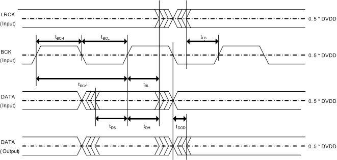 Figure 2. PCM514x Serial Audio Timing - Slave
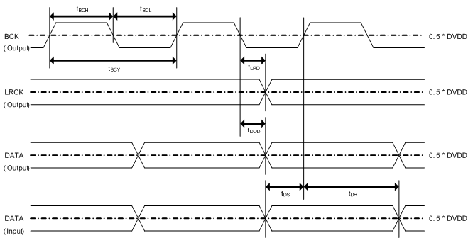 Figure 3. PCM514x Serial Audio Timing - I2S Master
 Figure 4. XSMT Timing for Soft Mute and Soft Un-Mute
7.11 Typical Characteristics
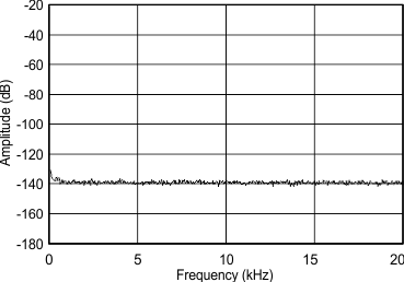
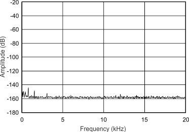
Consumer grade (non-Q1) devices are specified for TA = 25°C, AVDD = CPVDD = DVDD = 3.3 V, fS = 48 kHz, system clock = 512 fS and 24-bit data (unless otherwise noted).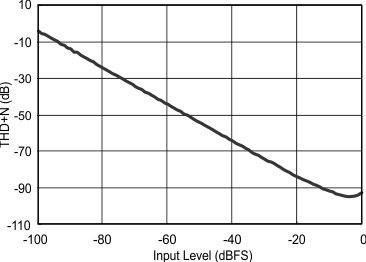
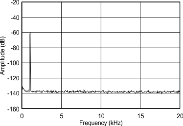
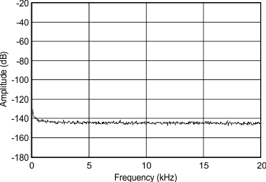
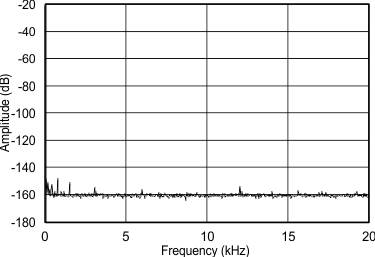
(–60 dBFS) from DC to 20 kHz
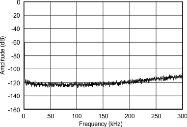
(–60 dBFS) from DC to 300 kHz
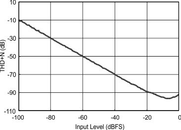
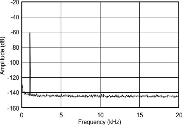
(–60 dBFS) from DC to 20 kHz
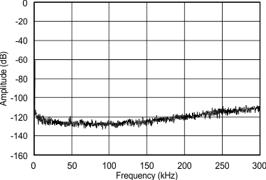
(–60 dBFS) from DC to 300 kHz