ZHCS688I November 2011 – March 2018 TPS65217
PRODUCTION DATA.
- 1 特性
- 2 应用
- 3 说明
- 4 修订历史记录
- 5 Device Comparison Table
- 6 Pin Configuration and Functions
- 7 Specifications
-
8 Detailed Description
- 8.1 Overview
- 8.2 Functional Block Diagram
- 8.3
Feature Description
- 8.3.1 Wake-Up and Power-Up Sequencing
- 8.3.2 Power Good
- 8.3.3 Push-Button Monitor (PB_IN)
- 8.3.4 nWAKEUP Pin (nWAKEUP)
- 8.3.5 Power Enable Pin (PWR_EN)
- 8.3.6 Reset Pin (nRESET)
- 8.3.7 Interrupt Pin (nINT)
- 8.3.8 Analog Multiplexer
- 8.3.9 Battery Charger and Power Path
- 8.3.10 Battery Charging
- 8.3.11 Precharge
- 8.3.12 Charge Termination
- 8.3.13 Battery Detection and Recharge
- 8.3.14 Safety Timer
- 8.3.15 Battery-Pack Temperature Monitoring
- 8.3.16 DC/DC Converters
- 8.3.17 Standby LDO Regulators (LDO1, LDO2)
- 8.3.18 Load Switches or LDO Regulators (LS1 or LDO3, LS2 or LDO4)
- 8.3.19 White LED Driver
- 8.4 Device Functional Modes
- 8.5 Programming
- 8.6
Register Maps
- 8.6.1 Register Address Map
- 8.6.2 Chip ID Register (CHIPID) (Address = 0x00) [reset = X]
- 8.6.3 Power Path Control Register (PPATH) (Address = 0x01) [reset = 0x3D]
- 8.6.4 Interrupt Register (INT) (Address = 0x02) [reset = 0x80]
- 8.6.5 Charger Configuration Register 0 (CHGCONFIG0) (Address = 0x03) [reset = 0x00]
- 8.6.6 Charger Configuration Register 1 (CHGCONFIG1) (Address = 0x04) [reset = 0xB1]
- 8.6.7 Charger Configuration Register 2 (CHGCONFIG2) (Address = 0x05) [reset = 0x80]
- 8.6.8 Charger Configuration Register 3 (CHGCONFIG3) (Address = 0x06) [reset = 0xB2]
- 8.6.9 WLED Control Register 1 (WLEDCTRL1) (Address = 0x07) [reset = 0xB1]
- 8.6.10 WLED Control Register 2 (WLEDCTRL2) (Address = 0x08) [reset = 0x00]
- 8.6.11 MUX Control Register (MUXCTRL) (Address = 0x09) [reset = 0x00]
- 8.6.12 Status Register (STATUS) (Address = 0x0A) [reset = 0x00]
- 8.6.13 Password Register (PASSWORD) (Address = 0x0B) [reset = 0x00]
- 8.6.14 Power Good Register (PGOOD) (Address = 0x0C) [reset = 0x00]
- 8.6.15 Power-Good Control Register (DEFPG) (Address = 0x0D) [reset = 0x0C]
- 8.6.16 DCDC1 Control Register (DEFDCDC1) (Address = 0x0E) [reset = X]
- 8.6.17 DCDC2 Control Register (DEFDCDC2) (Address = 0x0F) [reset = X]
- 8.6.18 DCDC3 Control Register (DEFDCDC3) (Address = 0x10) [reset = 0x08]
- 8.6.19 Slew-Rate Control Register (DEFSLEW) (Address = 0x11) [reset = 0x06]
- 8.6.20 LDO1 Control Register (DEFLDO1) (Address = 0x12) [reset = 0x09]
- 8.6.21 LDO2 Control Register (DEFLDO2) (Address = 0x13) [reset = 0x38]
- 8.6.22 Load Switch1 or LDO3 Control Register (DEFLS1) (Address = 0x14) [reset = X]
- 8.6.23 Load Switch2 or LDO4 Control Register (DEFLS2) (Address = 0x15) [reset = X]
- 8.6.24 Enable Register (ENABLE) (Address = 0x16) [reset = 0x00]
- 8.6.25 UVLO Control Register (DEFUVLO) (Address = 0x18) [reset = 0x03]
- 8.6.26 Sequencer Register 1 (SEQ1) (Address = 0x19) [reset = X]
- 8.6.27 Sequencer Register 2 (SEQ2) (Address = 0x1A) [reset = X]
- 8.6.28 Sequencer Register 3 (SEQ3) (Address = 0x1B) [reset = X]
- 8.6.29 Sequencer Register 4 (SEQ4) (Address = 0x1C) [reset = 0x40]
- 8.6.30 Sequencer Register 5 (SEQ5) (Address = 0x1D) [reset = X]
- 8.6.31 Sequencer Register 6 (SEQ6) (Address = 0x1E) [reset = 0x00]
- 9 Application and Implementation
- 10Power Supply Recommendations
- 11Layout
- 12器件和文档支持
- 13机械、封装和可订购信息
8.3.3 Push-Button Monitor (PB_IN)
The TPS65217x device has an active-low PB_IN input pin that is typically connected to ground through a push-button switch. The PB_IN input has a 50-ms deglitch time and an internal pull-up resistor that is connected to an always-on supply. The always-on supply is an unregulated internal power rail that is functionally equivalent to the power path. The source of the always-on supply is the same as the source of the SYS pin. The push-button monitor has two functions. The first is to power-up the device from the OFF or SLEEP state when a falling edge is detected on the PB_IN pin. The second is to power cycle the device when the PB_IN pin is held low for more than 8 s.
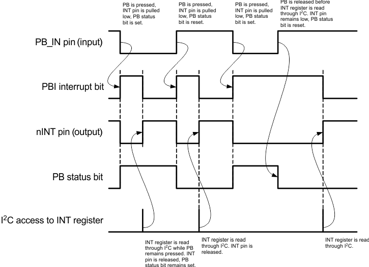
For a description of each function, see the Device Functional Modes section. A change in push-button status (the PB_IN pin goes from high to low or low to high) is signaled to the host through the PBI interrupt bit in the INT register. The current status of the interrupt can be checked by reading the PB status bit in the STATUS register. Figure 8 shows a timing diagram for the push-button monitor.
 Figure 8. Timing Diagram of the Push-Button Monitor Circuit