ZHCSDD8D October 2014 – December 2019 TPS1H100-Q1
PRODUCTION DATA.
- 1 特性
- 2 应用
- 3 说明
- 4 修订历史记录
- 5 Pin Configuration and Functions
- 6 Specifications
-
7 Detailed Description
- 7.1 Overview
- 7.2 Functional Block Diagram
- 7.3
Feature Description
- 7.3.1 Accurate Current Sense
- 7.3.2 Programmable Current Limit
- 7.3.3 Inductive-Load Switching-Off Clamp
- 7.3.4
Full Protections and Diagnostics
- 7.3.4.1 Short-to-GND and Overload Detection
- 7.3.4.2 Open-Load Detection
- 7.3.4.3 Short-to-Battery Detection
- 7.3.4.4 Reverse-Polarity Detection
- 7.3.4.5 Thermal Protection Behavior
- 7.3.4.6 UVLO Protection
- 7.3.4.7 Loss of GND Protection
- 7.3.4.8 Loss of Power Supply Protection
- 7.3.4.9 Reverse Current Protection
- 7.3.4.10 Protection for MCU I/Os
- 7.3.5 Diagnostic Enable Function
- 7.4 Device Functional Modes
- 8 Application and Implementation
- 9 Power Supply Recommendations
- 10Layout
- 11器件和文档支持
- 12机械、封装和可订购信息
7.3.3 Inductive-Load Switching-Off Clamp
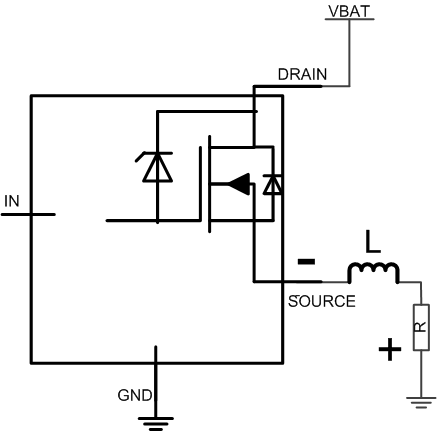
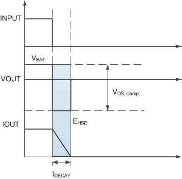
When an inductive load is switching off, the output voltage is pulled down to negative, due to the inductance characteristics. The power FET may break down if the voltage is not clamped during the current-decay period. To protect the power FET in this situation, internally clamp the drain-to-source voltage, namely VDS,clamp, the clamp diode between the drain and gate.

During the current-decay period (TDECAY), the power FET is turned on for inductance-energy dissipation. Both the energy of the power supply (EBAT) and the load (ELOAD) are dissipated on the high-side power switch itself, which is called EHSD. If resistance is in series with inductance, some of the load energy is dissipated in the resistance.

From the high-side power switch’s view, EHSD equals the integration value during the current-decay period.


When R approximately equals 0, EHSD can be given simply as:

 Figure 32. Driving Inductive Load
  Figure 33. Inductive-Load Switching-Off Diagram
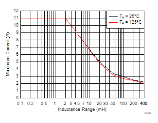
 As discussed previously, when switching off, battery energy and load energy are dissipated on the high-side power switch, which leads to the large thermal variation. For each high-side power switch, the upper limit of the maximum safe power dissipation depends on the device intrinsic capacity, ambient temperature, and board dissipation condition. TI provides the upper limit of single-pulse energy that devices can tolerate under the test condition: VVS = 13.5 V, inductance from 0.1 mH to 400 mH, R = 0 Ω, FR4 2s2p board, 2- × 70-μm copper, 2- × 35-μm copper, thermal pad copper area 600 mm2.
For one dedicated inductance, see Figure 34. If the maximum switching-off current is lower than the current value shown on the curve, the internal clamp function can be used for the demagnetization energy dissipation. If not, external free-wheeling circuitry is necessary for device protection.
