ZHCSEV7I June   2011  – October 2019 LM5113

PRODUCTION DATA.  

  1. 特性
  2. 应用
  3. 说明
    1.     Device Images
      1.      简化应用示意图
  4. 修订历史记录
  5. Pin Configuration and Functions
    1.     Pin Functions
  6. Specifications
    1. 6.1 Absolute Maximum Ratings
    2. 6.2 ESD Ratings
    3. 6.3 Recommended Operating Conditions
    4. 6.4 Thermal Information
    5. 6.5 Electrical Characteristics
    6. 6.6 Switching Characteristics
    7. 6.7 Typical Characteristics
  7. Detailed Description
    1. 7.1 Overview
    2. 7.2 Functional Block Diagram
    3. 7.3 Feature Description
      1. 7.3.1 Input and Output
      2. 7.3.2 Start-Up and UVLO
      3. 7.3.3 HS Negative Voltage and Bootstrap Supply Voltage Clamping
      4. 7.3.4 Level Shift
    4. 7.4 Device Functional Modes
  8. Application and Implementation
    1. 8.1 Application Information
    2. 8.2 Typical Application
      1. 8.2.1 Design Requirements
      2. 8.2.2 Detailed Design Procedure
        1. 8.2.2.1 VDD Bypass Capacitor
        2. 8.2.2.2 Bootstrap Capacitor
        3. 8.2.2.3 Power Dissipation
      3. 8.2.3 Application Curves
  9. Power Supply Recommendations
  10. 10Layout
    1. 10.1 Layout Guidelines
    2. 10.2 Layout Examples
  11. 11器件和文档支持
    1. 11.1 文档支持
      1. 11.1.1 相关文档
    2. 11.2 支持资源
    3. 11.3 商标
    4. 11.4 静电放电警告
    5. 11.5 Glossary
  12. 12机械、封装和可订购信息

Application Curves

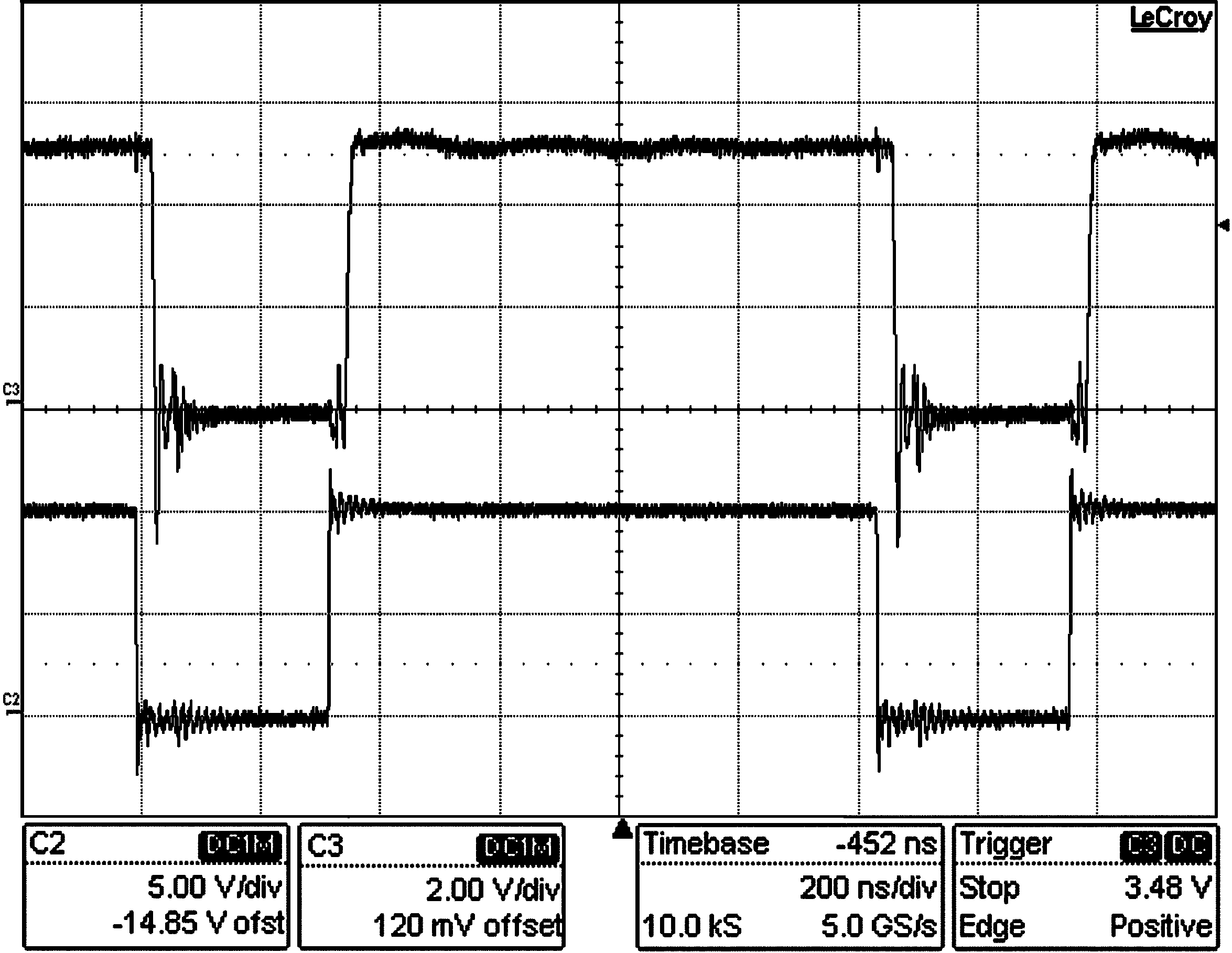
LM5113 30163005.png
Conditions:
Input Voltage = 48 V DC, Load Current = 5 A
Traces:
Top Trace: Gate of Low-Side eGaN FET, Volt/div = 2 V
Bottom Trace: LI of LM5113, Volt/div = 5 V
Bandwidth Limit = 600 MHz
Horizontal Resolution = 0.2 µs/div
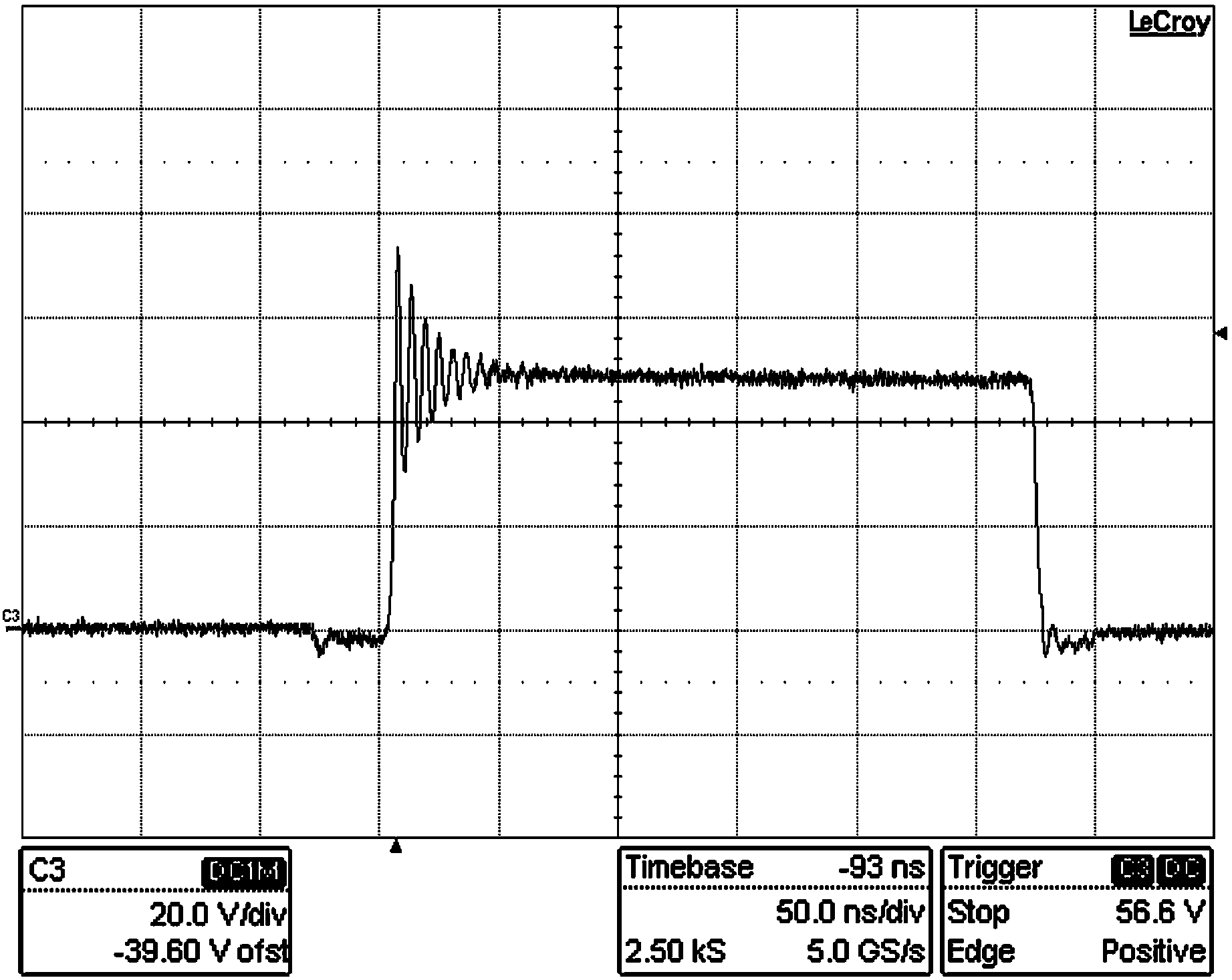
Figure 22. Low-Side Driver Input and Output
LM5113 30163006.png
Conditions:
Input Voltage = 48 V DC,
Load Current = 10 A
Traces:
Trace: Switch-Node Voltage, Volts/div = 20 V
Bandwidth Limit = 600 MHz
Horizontal Resolution = 50 ns/div
Figure 23. Switch-Node Voltage