ZHCSF55E June 2016 – December 2021 UCC21520
PRODUCTION DATA
- 1 特性
- 2 应用
- 3 说明
- 4 Revision History
- 5 说明(续)
- 6 Pin Configuration and Functions
-
7 Specifications
- 7.1 Absolute Maximum Ratings
- 7.2 ESD Ratings
- 7.3 Recommended Operating Conditions
- 7.4 Thermal Information
- 7.5 Power Ratings
- 7.6 Insulation Specifications
- 7.7 Safety-Related Certifications
- 7.8 Safety-Limiting Values
- 7.9 Electrical Characteristics
- 7.10 Switching Characteristics
- 7.11 Insulation Characteristics Curves
- 7.12 Typical Characteristics
- 8 Parameter Measurement Information
- 9 Detailed Description
-
10Application and Implementation
- 10.1 Application Information
- 10.2
Typical Application
- 10.2.1 Design Requirements
- 10.2.2
Detailed Design Procedure
- 10.2.2.1 Designing INA/INB Input Filter
- 10.2.2.2 Select External Bootstrap Diode and its Series Resistor
- 10.2.2.3 Gate Driver Output Resistor
- 10.2.2.4 Gate to Source Resistor Selection
- 10.2.2.5 Estimate Gate Driver Power Loss
- 10.2.2.6 Estimating Junction Temperature
- 10.2.2.7 Selecting VCCI, VDDA/B Capacitor
- 10.2.2.8 Dead Time Setting Guidelines
- 10.2.2.9 Application Circuits with Output Stage Negative Bias
- 10.2.3 Application Curves
- 11Power Supply Recommendations
- 12Layout
- 13Device and Documentation Support
- 14Mechanical, Packaging, and Orderable Information
7.12 Typical Characteristics
VDDA = VDDB= 12 V, VCCI = 3.3 V, TA = 25°C, No load unless otherwise noted.
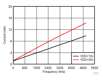 Figure 7-4 Per Channel Current Consumption vs Frequency (No Load, VDD = 12 V or 25 V)
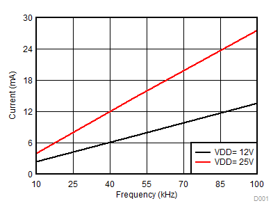 Figure 7-6 Per Channel Current Consumption (IVDDA/B) vs Frequency (10-nF Load, VDD = 12 V or 25 V)
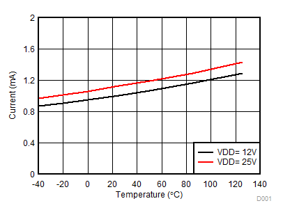 Figure 7-8 Per Channel (IVDDA/B) Quiescent Supply Current vs Temperature (No Load, Input Low, No Switching)
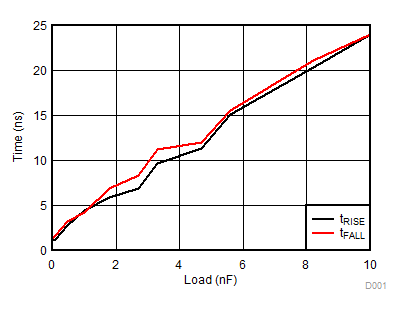 Figure 7-10 Rising and Falling Times vs Load (VDD = 12 V)
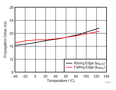 Figure 7-12 Propagation Delay vs Temperature
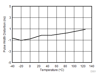 Figure 7-14 Pulse Width Distortion vs Temperature
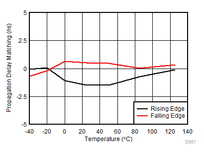 Figure 7-16 Propagation Delay Matching (tDM) vs Temperature
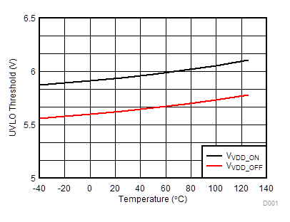 Figure 7-18 VDD 5-V UVLO Threshold vs Temperature
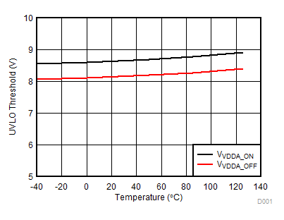 Figure 7-20 VDD 8-V UVLO Threshold vs Temperature
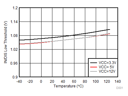 Figure 7-22 IN/DIS Low Threshold
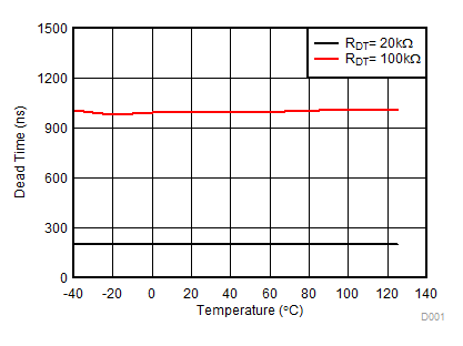 Figure 7-24 Dead Time vs Temperature (with RDT = 20 kΩ and 100 kΩ)
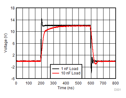 Figure 7-26 Typical Output Waveforms
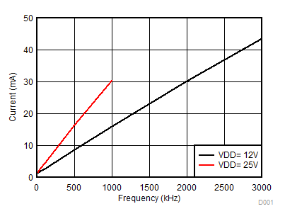 Figure 7-5 Per Channel Current Consumption (IVDDA/B) vs Frequency (1-nF Load, VDD = 12 V or 25 V)
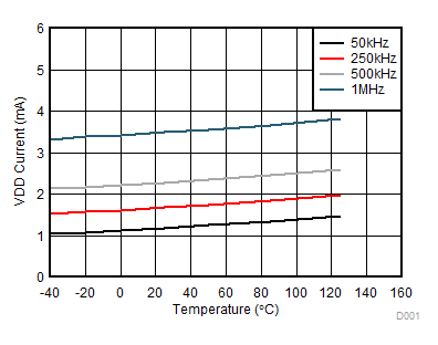 Figure 7-7 Per Channel (IVDDA/B) Supply Current Vs. Temperature (No Load, Different Switching Frequencies)
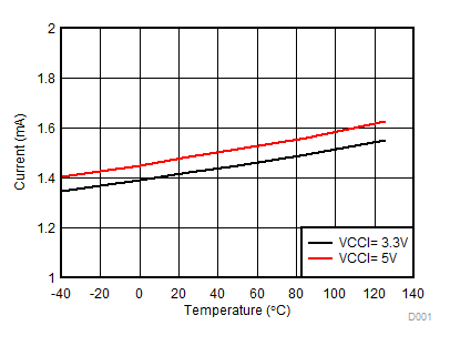 Figure 7-9 IVCCI Quiescent Supply Current vs Temperature (No Load, Input Low, No Switching)
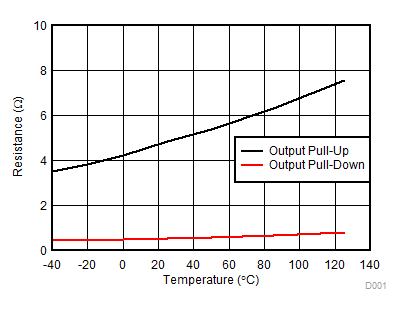 Figure 7-11 Output Resistance vs Temperature
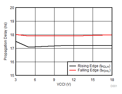 Figure 7-13 Propagation Delay vs VCCI
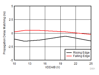 Figure 7-15 Propagation Delay Matching (tDM) vs VDD
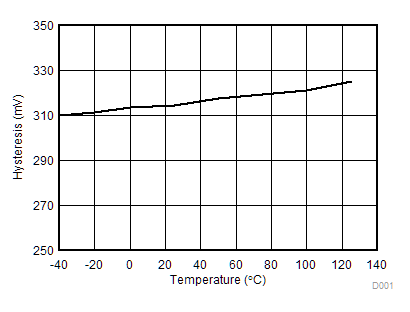 Figure 7-17 VDD 5-V UVLO Hysteresis vs Temperature
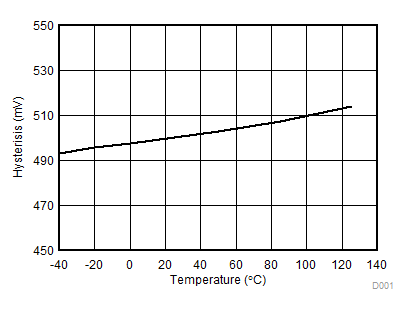 Figure 7-19 VDD 8-V UVLO Hysteresis vs Temperature
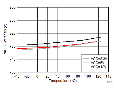 Figure 7-21 IN/DIS Hysteresis vs Temperature
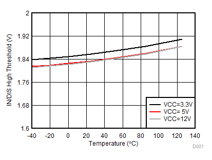 Figure 7-23 IN/DIS High Threshold
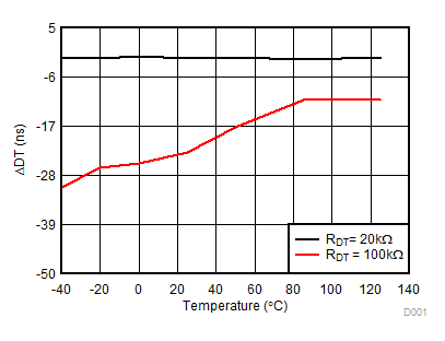 Figure 7-25 Dead Time Matching vs Temperature (with RDT = 20 kΩ and 100 kΩ)