ZHCSGB0B November 2017 – November 2020 LM5145
PRODUCTION DATA
- 1 特性
- 2 应用
- 3 说明
- 4 Revision History
- 5 Description (continued)
- 6 Pin Configuration and Functions
- 7 Specifications
-
8 Detailed Description
- 8.1 Overview
- 8.2 Functional Block Diagram
- 8.3
Feature Description
- 8.3.1 Input Range (VIN)
- 8.3.2 Output Voltage Setpoint and Accuracy (FB)
- 8.3.3 High-Voltage Bias Supply Regulator (VCC)
- 8.3.4 Precision Enable (EN/UVLO)
- 8.3.5 Power Good Monitor (PGOOD)
- 8.3.6 Switching Frequency (RT, SYNCIN)
- 8.3.7 Configurable Soft Start (SS/TRK)
- 8.3.8 Voltage-Mode Control (COMP)
- 8.3.9 Gate Drivers (LO, HO)
- 8.3.10 Current Sensing and Overcurrent Protection (ILIM)
- 8.3.11 OCP Duty Cycle Limiter
- 8.4 Device Functional Modes
-
9 Application and Implementation
- 9.1 Application Information
- 9.2
Typical Applications
- 9.2.1 Design 1 – 20-A High-Efficiency Synchronous Buck Regulator for Telecom Power Applications
- 9.2.2 Design 2 – High Density, 12-V, 10-A Rail With LDO Low-Noise Auxiliary Output for RF Power Applications
- 9.2.3 Design 3 – 150-W, Regulated 24-V Rail for Commercial Drone Applications With Output Voltage Tracking Feature
- 9.2.4 Design 4 – Powering a Multicore DSP From a 24-V or 48-V Rail
- 10Power Supply Recommendations
- 11Layout
- 12Device and Documentation Support
- 13Mechanical, Packaging, and Orderable Information
8.3.11 OCP Duty Cycle Limiter
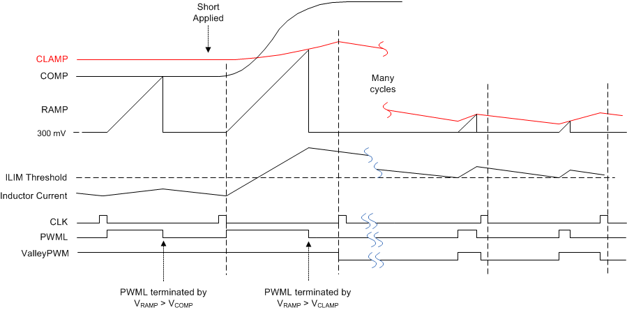
 Figure 8-11 OCP Duty Cycle Limiting Waveforms
In addition to valley current limiting, the LM5145 uses a proprietary duty-cycle limiter circuit to reduce the PWM on-time during an overcurrent condition. As shown in Figure 8-10, an auxiliary PWM comparator along with a modulated CLAMP voltage limits how quickly the on-time increases in response to a large step in the COMP voltage that typically occurs with a voltage-mode control loop architecture.
As depicted in Figure 8-11, the CLAMP voltage, VCLAMP, is normally regulated above the COMP voltage to provide adequate headroom during a response to a load-on transient. If the COMP voltage rises quickly during an overloaded or shorted output condition, the on-time pulse terminates thereby limiting the on-time and peak inductor current. Moreover, the CLAMP voltage is reduced if additional valley current limit events occur, further reducing the average output current. If the overcurrent condition exists for 128 continuous clock cycles, a hiccup event is triggered and SS is pulled low for 8192 clock cycles before a soft-start sequence is initiated.