ZHCSGF6A April 2017 – July 2017 TPD2S701-Q1
PRODUCTION DATA.
- 1 特性
- 2 应用
- 3 说明
- 4 修订历史
- 5 Pin Configuration and Functions
-
6 Specifications
- 6.1 Absolute Maximum Ratings
- 6.2 ESD Ratings—AEC Specification
- 6.3 ESD Ratings—IEC Specification
- 6.4 ESD Ratings—ISO Specification
- 6.5 Recommended Operating Conditions
- 6.6 Thermal Information
- 6.7 Electrical Characteristics
- 6.8 Power Supply and Supply Current Consumption Chracteristics
- 6.9 Timing Requirements
- 6.10 Typical Characteristics
- 7 Parameter Measurement Information
- 8 Detailed Description
- 9 Application and Implementation
- 10Power Supply Recommendations
- 11Layout
- 12器件和文档支持
- 13机械、封装和可订购信息
8 Detailed Description
8.1 Overview
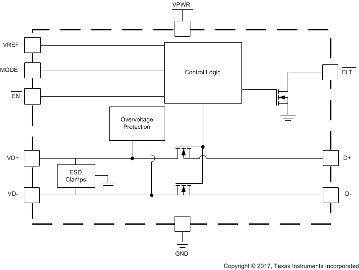
The TPD2S701-Q1 is a 2-Channel Data Line Short-to-VBUS and IEC61000-4-2 ESD protection device for automotive high-speed interfaces like USB2.0. The TPD2S701-Q1 contains two data line nFET switches which ensure safe data communication while protecting the internal system circuits from any overvoltage conditions at the VD+ and VD– pins. On these pins, this device can handle overvoltage protection up to 7-V DC. This provides sufficient protection for shorting the data lines to the USB VBUS rail.
Additionally, the TPD2S701-Q1 has a FLT pin which provides an indication when the device sees an overvoltage condition and automatically resets when the overvoltage condition is removed. The TPD2S701-Q1 also integrates IEC ESD clamps on the VD+ and VD– pins, thus eliminating the need for external TVS clamp circuits in the application.
The TPD2S701-Q1 has an internal oscillator and charge pump that controls the turnon of the internal nFET switches. The internal oscillator controls the timers that enable the charge pump and resets the open-drain FLT output. If VD+ and VD– are less than VOVP, the internal charge pump is enabled. After an internal delay, the charge-pump starts-up, turning on the internal nFET switches. At any time, if VD+ or VD– rises above VOVP, TPD2S701-Q1 asserts FLT pin LOW and the nFET switches are turned off.
8.2 Functional Block Diagram

8.3 Feature Description
8.3.1 OVP Operation
When the VD+, or VD– voltages rise above VOVP, the internal nFET switches are turned off, protecting the transceiver from overvoltage conditions. The response is very rapid, with the FET switches turning off in less than 1 µs. Before the OVP condition, the FLT pin is High-Z, and is pulled HIGH via an external resistor to indicate there is no fault. Once the OVP condition occurs, the FLT pin is asserted LOW. When the VD+, or VD– voltages returns below VOVP – VHYS-OVP, the nFET switches are turned on again. When the OVP condition is cleared and the nFETs are completely turned on, the FLT is reset to high-Z.
8.3.2 OVP Threshold
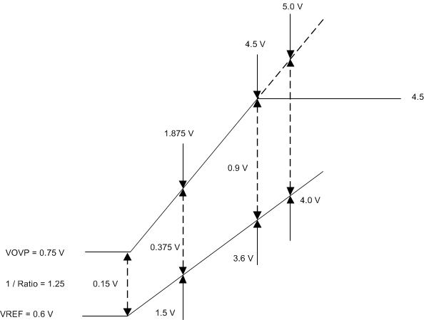
 Figure 20. OVP Threshold
The OVP Threshold VOVP is set by VREF according to Equation 1, Equation 2 and Equation 3.


Equation 1, Equation 2 and Equation 3 yield the typical VOVP values. See the parametric tables for the minimum and maximum values that include variation over temperature and process. Figure 20 gives a graphical representation of the relationship between VOVP and VREF.
VREF can be set either by an external regulator (Mode 0) or an internal adjustable regulator (Mode 1). See the VREF Operation section for more details on how to operate VREF in Mode 0 and Mode 1.
8.3.3 D± Clamping Voltage
The TPD2S701-Q1 provides a differentiated device architecture which allows the system designer to control the clamping voltage the protected transceiver sees from the D+ and D– pins. This architecture allows the system designer to minimize the amount of stress the transceiver sees during ESD events. The clamping voltage that appears on the D+ and D– lines during an ESD event obeys Equation 4.

Where VBR approximately = 0.7 V, IRDYN approximately = 1 V. By adjusting VREF, the clamping voltage of the D+ and D– lines can be adjusted. As VREF also controls the OVP threshold, take care to insure that the VREF setting both satisfies the OVP threshold requirements while simultaneously optimizing system protection on the D+ and D– lines.
The size of the capacitor used on the VREF pin also influences the clamping voltage as transient currents during ESD events flow into the VREF capacitor. This causes the VREF voltage to increase, and likewise the clamping voltage on D± according to Equation 4. The larger capacitor that is used, the better the clamping performance of the device is going to be. See the parametric tables for the clamping performance of the TPD2S701-Q1 with a 1-µF capacitor.
8.4 Device Functional Modes
The TPD2S701-Q1 has two modes of operation which vary the way the VREF pin functions. In Mode 0, the VREF pin is connected to an external regulator which sets the voltage on the VREF pin. In Mode 1, the TPD2S701-Q1 uses an adjustable internal regulator to set the VREF voltage. Mode 1 enables the system designer to operate the TPD2S701-Q1 with a single power supply, and have the flexibility to easily set the VREF voltage to any voltage between 0.6 V and 3.8 V with two external resistors.