ZHCSH68F November 2017 – February 2024 UCC21220 , UCC21220A
PRODUCTION DATA
- 1
- 1 特性
- 2 应用
- 3 说明
- 4 Device Comparison Table
- 5 Pin Configuration and Functions
-
6 Specifications
- 6.1 Absolute Maximum Ratings
- 6.2 ESD Ratings
- 6.3 Recommended Operating Conditions
- 6.4 Thermal Information
- 6.5 Power Ratings
- 6.6 Insulation Specifications
- 6.7 Safety-Related Certifications
- 6.8 Safety-Limiting Values
- 6.9 Electrical Characteristics
- 6.10 Switching Characteristics
- 6.11 Thermal Derating Curves
- 6.12 Typical Characteristics
- 7 Parameter Measurement Information
- 8 Detailed Description
-
9 Application and Implementation
- 9.1 Application Information
- 9.2
Typical Application
- 9.2.1 Design Requirements
- 9.2.2
Detailed Design Procedure
- 9.2.2.1 Designing INA/INB Input Filter
- 9.2.2.2 Select External Bootstrap Diode and its Series Resistor
- 9.2.2.3 Gate Driver Output Resistor
- 9.2.2.4 Estimating Gate Driver Power Loss
- 9.2.2.5 Estimating Junction Temperature
- 9.2.2.6 Selecting VCCI, VDDA/B Capacitor
- 9.2.2.7 Application Circuits with Output Stage Negative Bias
- 9.2.3 Application Curves
- 10Power Supply Recommendations
- 11Layout
- 12Device and Documentation Support
- 13Revision History
- 14Mechanical, Packaging, and Orderable Information
8.3.4 Output Stage
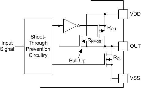
The UCC21220 and UCC21220A output stages feature a pull-up structure which delivers the highest peak-source current when it is most needed, during the Miller plateau region of the power-switch turn on transition (when the power switch drain or collector voltage experiences dV/dt). The output stage pull-up structure features a P-channel MOSFET and an additional Pull-Up N-channel MOSFET in parallel. The function of the N-channel MOSFET is to provide a boost in the peak-sourcing current, enabling fast turn on. This is accomplished by briefly turning on the N-channel MOSFET during a narrow instant when the output is changing states from low to high. The on-resistance of this N-channel MOSFET (RNMOS) is approximately 1.47 Ω when activated.
The ROH parameter is a DC measurement and it is representative of the on-resistance of the P-channel device only. This is because the Pull-Up N-channel device is held in the off state in DC condition and is turned on only for a brief instant when the output is changing states from low to high. Therefore the effective resistance of the UCC21220 and UCC21220A pull-up stage during this brief turn-on phase is much lower than what is represented by the ROH parameter.
The pull-down structure of the UCC21220 and UCC21220A are composed of an N-channel MOSFET. The ROL parameter, which is also a DC measurement, is representative of the impedance of the pull-down state in the device. Both outputs of the UCC21220 and UCC21220A are capable of delivering 4-A peak source and 6-A peak sink current pulses. The output voltage swings between VDD and VSS provides rail-to-rail operation, thanks to the MOS-out stage which delivers very low drop-out.
 Figure 8-2 Output Stage