ZHCSHX8D September 2017 – October 2019 TPS50601A-SP
PRODUCTION DATA.
- 1 特性
- 2 应用
- 3 说明
- 4 修订历史记录
- 5 Pin Configuration and Functions
- 6 Specifications
-
7 Detailed Description
- 7.1 Overview
- 7.2 Functional Block Diagram
- 7.3
Feature Description
- 7.3.1 VIN and Power VIN Pins (VIN and PVIN)
- 7.3.2 Voltage Reference
- 7.3.3 Adjusting the Output Voltage
- 7.3.4 Safe Start-Up Into Prebiased Outputs
- 7.3.5 Error Amplifier
- 7.3.6 Slope Compensation
- 7.3.7 Enable and Adjust UVLO
- 7.3.8 Adjustable Switching Frequency and Synchronization (SYNC)
- 7.3.9 Slow Start (SS/TR)
- 7.3.10 Power Good (PWRGD)
- 7.3.11 Sequencing (SS/TR)
- 7.3.12 Output Overvoltage Protection (OVP)
- 7.3.13 Overcurrent Protection
- 7.3.14 Thermal Shutdown
- 7.3.15 Turn-On Behavior
- 7.3.16 Small Signal Model for Frequency Compensation
- 7.4 Device Functional Modes
- 8 Application and Implementation
- 9 Power Supply Recommendations
- 10Layout
- 11器件和文档支持
- 12机械、封装和可订购信息
8.2.3 Parallel Operation
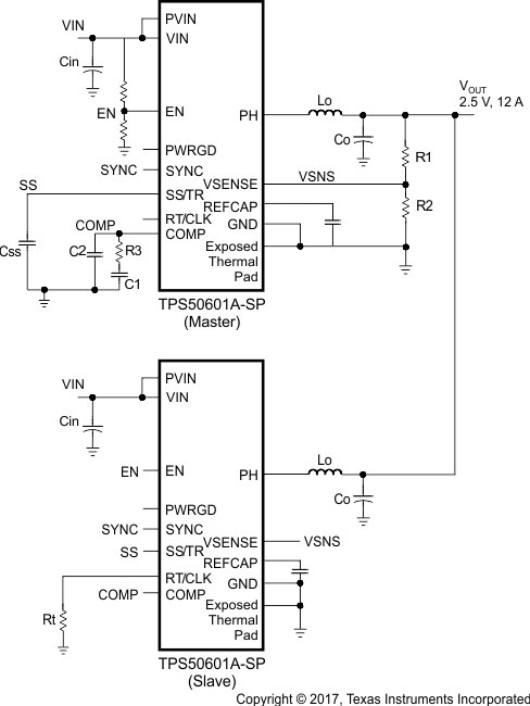
The TPS50601A-SP can be configured in master-slave mode to provide 12-A output current as shown in Figure 24.
 Figure 24. Parallel Configuration Showing Master and Slave
 The design procedure to configure the master-slave operation using the internal oscillator is as follows:
- The RT pin of the master device must be left floating. This achieves 2 purposes, to set the frequency to 500 kHz (typical) using the internal oscillator and to configure the SYNC pin of the master device as an output pin with a 500-kHz clock, 180° in phase respect to the internal oscillator of the master device. For more details, see Adjustable Switching Frequency and Synchronization (SYNC) section.
- The RT pin on slave device should be connected to a resistor such that the frequency of the slave device is within 5% of the master's frequency, 500 kHz in this case. See Figure 18 for reference.
- SYNC pin of the master device must be connected to the SYNC pin of the slave device.
- Only a single feedback network is needed connected to the VSENSE pin of the master device. Therefore, both VSENSE pins must be connected.
- Only a single compensation network is needed connected to the COMP pin of the master device. Therefore both COMP pins must be connected.
- Only a single soft start capacitor is needed connected to the SS pin of the master device. Therefore both SS pins must be connected.
- Only a single enable signal (or resistor divider) is needed connected to the EN pin of the master device. Therefore, both EN pins must be connected.
- Since the master device controls the compensation, soft start and enable networks, the factor of 2 must be taken into account when calculating the components associated with these pins.
The master-slave mode can also be implemented using an external clock. In such case, a different frequency other than 500 kHz can be used. When using an external clock, only the RT and SYNC pins configuration varies as follows:
- RT pins of both master and slave device must be connected to a resistor matching the frequency of the external clock being used. See Figure 18 for reference.
- The external clock is connected to the SYNC pin of the master device. A 10-kΩ resistor to GND should be connected to the SYNC pin as well.
- An inverted clock (180° in phase respect to the master device) must be connected to the SYNC pin of the slave device. A 10-kΩ resistor to GND should be connected to the SYNC pin as well.