ZHCSIL2C July 2018 – March 2022 UCC24624
PRODUCTION DATA
- 1 特性
- 2 应用
- 3 说明
- 4 Revision History
- 5 说明(续)
- 6 Pin Configuration and Functions
- 7 Specifications
- 8 Detailed Description
- 9 Application and Implementation
- 10Power Supply Recommendations
- 11Layout
- 12Device and Documentation Support
8.3.4.5 Adaptive Turn-on Delay
To further enhance noise immunity of the SR controller, UCC24624 implements an adaptive turn-on delay. During most operating conditions, 155-ns of turn-on delay is applied to both channel's turn-on stage. However, at a lighter load, or during burst off period, this turn-on delay is increased to further enhance the noise immunity and allow the controller to reject the leading edge current spike and DCM ring. In these conditions, the turn-on delay is increased to 275 ns. The turn-on delay increasing can be observed in below conditions.
- Burst mode operation. During LLC normal operation, two SR MOSFETs are turned on and off alternatively, in a complementary fashion. However, during burst operation, after one SR MOSFET turns off, the other SR MOSFET stays off. This gives the indication of the LLC converter entering the burst-mode operation. In UCC24624, after one channel SR is turned off, its turn-on delay for the next turn-on is increased to 275 ns, for improved DCM ring rejection capability. If the other channel SR is turned on after this channel SR turning off, the LLC is still in normal operating mode. The turn-on delay is reset to the 155-ns value. Otherwise, UCC24624 detects the LLC entering burst-mode operation and the SR turn-on delay stays at 275 ns to help reject the DCM ring. This adaptive turn-on delay allows long turn-on delay during burst mode operation, with shorter delay during normal operation to minimize the conduction loss.
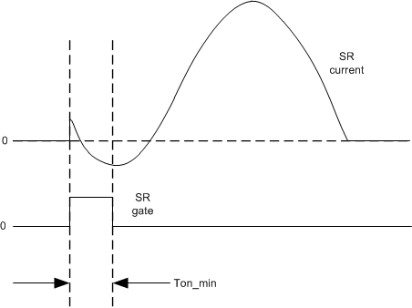
- Short SR conduction time. At light load, the SR current could start with a short leading edge spike of positive current, followed by the negative current, and then the full positive current, as shown in Figure 8-8. This is caused by the SR parasitic capacitance and the LLC resonant behavior. When the negative current appears, the SR is turned off with minimum on time (on-time blanking). This is the indication that the leading edge current spike causes abnormal operation. Once the short SR conduction time is detected, the IC sets the turn-on delay to 275 ns. This long turn-on delay can further help to reject the leading edge current spike. It also helps to provide better DCM ring rejection during burst mode operation, since the burst mode operation only happens at light load. This increased turn-on delay time is reset when the SR voltage drop is more than 40 mV (VDS more negative than -40 mV) at the middle of its conduction time for 8 consecutive cycles.
 Figure 8-8 SR current with leading edge spike
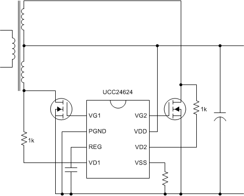
To avoid the DCM ring turn on and SR leading edge current spike, an extra resistor can be added between the SR MOSFET drain and UCC24624 VD pins, as shown in Figure 8-9. The extra resistor helps to further improve the noise immunity. Furthermore, this resistor also limits the negative current flowing into the VD pins, during SR body diode conduction time. A resistor value around 1 kΩ is recommended if this resistor is needed.
 Figure 8-9 UCC24624 configuration with VD resistors